Introduction
Delamination in PCB lamination represents one of the most serious defects in multilayer printed circuit board production. It occurs when the bond between copper foil, prepreg, or core layers fails, leading to separation that undermines structural integrity and electrical performance. This issue arises primarily during the high-temperature, high-pressure lamination cycle where materials must achieve uniform adhesion. Factory engineers encounter PCB delamination as a frequent cause of yield loss, often traced back to process variations or material conditions. Understanding its mechanisms allows for targeted interventions that enhance reliability in demanding applications. This article explores the causes of delamination, reliable detection methods, and proven prevention strategies aligned with industry practices.
What Is PCB Delamination and Why It Matters
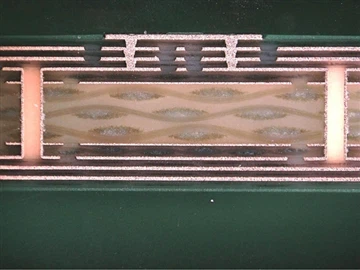
PCB delamination refers to the separation of layers within the laminate stackup, specifically at interfaces between resin, fiberglass, and copper. In the lamination process, prepreg sheets impregnated with partially cured resin bond multiple cores under controlled heat and pressure, forming a monolithic structure. Failure in this bonding results in voids, blisters, or full layer lift-off, classified as a PCB manufacturing defect. Laminate adhesion is crucial because delamination compromises signal integrity, introduces mechanical weaknesses, and accelerates failure under thermal cycling or vibration.
The consequences extend beyond initial production. Delaminated boards fail prematurely in assembly during reflow soldering or in field use under environmental stress. Electrical engineers designing high-density interconnects face risks of intermittent opens, increased impedance variations, and reduced thermal dissipation. According to acceptability criteria in IPC-A-600, delamination constitutes a rejectable condition that demands process corrections. Addressing it early prevents costly rework and ensures compliance with performance specifications. Ultimately, robust laminate adhesion safeguards long-term product reliability in sectors like telecommunications and automotive electronics.
Causes of Delamination in PCB Lamination
Moisture absorption stands as the leading cause of delamination, where absorbed water in prepreg or core materials vaporizes explosively during lamination temperatures exceeding 180 degrees Celsius. Hygroscopic resins draw ambient humidity, and if levels surpass 0.5 percent by weight, steam pressure disrupts interlayer bonds. Factory storage in uncontrolled environments exacerbates this, as laminates exposed to high relative humidity develop gradients that prevent uniform resin flow. Improper handling prior to layup compounds the issue, turning a preventable factor into a pervasive PCB manufacturing defect.
Contamination on copper surfaces or fiberglass contributes significantly to poor laminate adhesion. Dust, oils from handling, or residues from prior processes create barriers that inhibit resin wetting during pressing. In multilayer stacks, even microscopic particles at inner layers lead to localized delamination under pressure. Process engineers must recognize that surface energy mismatches from contaminants reduce peel strength, a key indicator of bond quality.
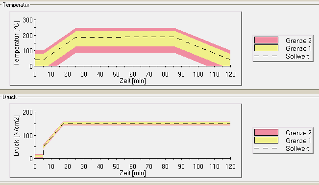
Incorrect lamination parameters trigger delamination through thermal or mechanical imbalances. Excessive ramp rates cause rapid resin gelation before full flow, trapping air or creating uneven curing. Insufficient pressure fails to expel volatiles, while overpressure induces microcracks in brittle resins. Material incompatibilities, such as mismatched glass transition temperatures between prepreg and core, amplify stress during cooldown, promoting separation.
Thermal mismatch between layers represents another mechanism, where differential expansion coefficients generate shear forces at interfaces. High-aspect-ratio stacks experience amplified effects, as edge constraints hinder uniform contraction. Factory data often links this to rapid cooling phases post-lamination, where residual stresses exceed adhesive limits.
Detecting Delamination in PCBs
Visual inspection serves as the first line of defense for detecting delamination, revealing surface blisters, white spots, or edge lift-off post-lamination. Engineers examine boards under high-intensity lighting or magnification for anomalies like weave exposure indicating resin starvation. While effective for gross defects, it misses subsurface issues common in thick multilayers. Combining it with thermal imaging highlights hot spots from poor thermal paths caused by separation.
Non-destructive ultrasonic testing provides precise detection of delamination through scanning acoustic microscopy or C-scan methods. Sound waves reflect differently at delaminated interfaces, producing echo maps that quantify void size and depth. This technique excels in production environments, allowing 100 percent inspection without compromising boards. Per test methods in IPC-TM-650, it correlates well with destructive verification.
Cross-sectioning offers definitive confirmation via metallographic preparation and microscopy. Slices through suspect areas expose interlayer gaps, measuring separation extent. Though destructive, it validates process data and supports root cause analysis. Electrical testing, such as continuity checks or impedance profiling, indirectly flags delamination by revealing opens or signal distortions.
X-ray inspection visualizes internal structures, identifying density variations from delamination. Real-time systems detect voids during inline quality control. Engineers integrate these methods hierarchically, starting with non-destructive for screening and escalating as needed.
Preventing Delamination: Best Practices in Manufacturing
Moisture management forms the cornerstone of preventing delamination, starting with controlled storage per J-STD-020 guidelines for moisture sensitivity. Bake laminates at 125 degrees Celsius for four hours to desorb absorbed water before layup, targeting less than 0.1 percent residual content. Use dry cabinets maintaining below 5 percent relative humidity, and handle materials with vacuum-sealed bags. Factory protocols include weight gain tests to verify dryness, ensuring no hygroscopic buildup.
Surface preparation enhances laminate adhesion by eliminating contaminants through plasma cleaning or chemical desmearing. Achieve surface energies above 50 dynes per centimeter for optimal resin bonding. Automated handling minimizes human-induced oils, while in-line verification confirms cleanliness.
Optimize lamination cycles with gradual ramps, holding at gelation temperature for full resin flow, followed by controlled pressure buildup. Profiles tailored to material specs, such as 20 to 30 minutes at peak temperature, expel volatiles effectively. Monitor press uniformity to avoid hotspots that induce uneven curing.
Material selection per IPC-6012 specifications ensures compatibility, favoring high-Tg resins for thermal stability. Verify peel strength exceeds minimums via qualification tests. Implement process controls like statistical process control on parameters to catch drifts early.
Regular audits and incoming inspections catch defects upstream. Train operators on handling, and maintain equipment calibration for presses and ovens.
Troubleshooting Common Delamination Scenarios
Engineers troubleshooting delamination often isolate moisture via bake trials on suspect lots. If symptoms persist post-baking, inspect for contamination through contact angle measurements. Parameter tweaks address thermal issues, with cycle simulations predicting outcomes.
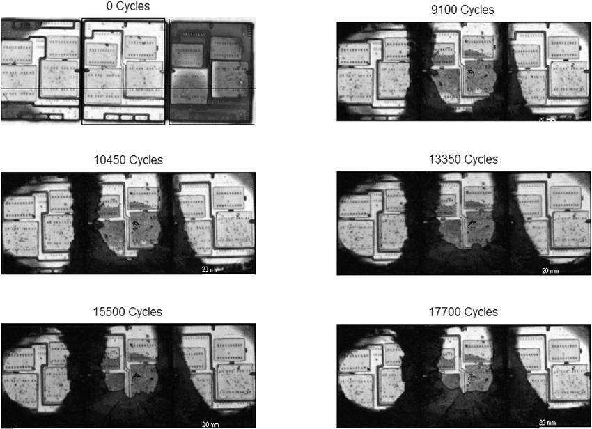
In high-layer-count boards, edge delamination signals pressure nonuniformity; adjust platens or foils accordingly. Post-lamination thermal shock tests per IPC-TM-650 reveal latent weaknesses early.
Conclusion
PCB delamination undermines laminate adhesion, stemming from moisture, contamination, and process flaws, yet systematic detection and prevention mitigate risks effectively. Ultrasonic and visual methods enable rapid identification, while moisture control and optimized cycles form robust defenses. Adhering to standards like IPC-A-600 ensures acceptability, bolstering manufacturing yields. Electric engineers benefit from these factory-driven insights, achieving reliable boards that withstand operational stresses. Proactive measures not only curb PCB manufacturing defects but also elevate overall quality.
FAQs
Q1: What are the primary causes of delamination in PCB lamination?
A1: Moisture absorption tops the list, as vaporization disrupts bonds during heat. Contamination hinders resin wetting, while improper temperature or pressure cycles cause uneven curing. Material mismatches add shear stresses. Factory controls targeting these yield significant reductions in defects.
Q2: How do you detect delamination without destroying the PCB?
A2: Scanning acoustic microscopy uses ultrasound to map internal separations non-destructively. X-ray reveals density changes, and visual checks spot surface signs. These methods integrate into production lines for efficient detecting delamination.
Q3: What steps prevent delamination during manufacturing?
A3: Bake materials to remove moisture per J-STD-020, clean surfaces rigorously, and fine-tune lamination profiles. Select compatible laminates and monitor processes continuously. These practices strengthen laminate adhesion and minimize PCB manufacturing defects.
Q4: Can delamination occur after lamination, and how to address it?
A4: Yes, thermal cycling or reflow can trigger latent delamination from residual stresses. Bake and re-laminate if feasible, or reject per IPC-A-600. Prevention via qualification testing avoids field failures.
References
IPC-6012E — Qualification and Performance Specification for Rigid Printed Boards. IPC, 2017
IPC-A-600K — Acceptability of Printed Boards. IPC, 2020
J-STD-020E — Moisture/Reflow Sensitivity Classification. JEDEC, 2014
IPC-TM-650 — Test Methods Manual. IPC, various


