Introduction
High-density printed circuit boards (PCBs) are the backbone of modern electronics, enabling compact designs with intricate functionality for devices ranging from smartphones to industrial controllers. However, the complexity of these boards poses significant challenges during assembly. Design for Assembly (DFA) is a critical methodology that focuses on simplifying the assembly process, reducing errors, and lowering production costs. For electrical engineers working on high-density PCBs, understanding DFA principles such as component placement, minimizing assembly steps, and optimizing for automated processes like pick and place systems is essential. This article explores key DFA considerations tailored for high-density PCBs, offering practical insights into fiducial markers, component layout strategies, and assembly efficiency. By integrating these practices, engineers can ensure smoother manufacturing and reliable end products.
What Is Design for Assembly (DFA) and Why It Matters
Design for Assembly refers to a set of design practices aimed at making the assembly of a product as efficient and error-free as possible. In the context of high-density PCBs, DFA becomes crucial due to the tight spacing, numerous components, and precision required during assembly. Poor DFA practices can lead to increased assembly time, higher defect rates, and elevated costs. For electrical engineers, applying DFA principles ensures that the board design aligns with the capabilities of automated assembly equipment and adheres to industry standards like those set by IPC. Effective DFA not only streamlines manufacturing but also enhances product reliability by reducing the likelihood of misalignment or soldering issues during production.
Technical Principles of DFA for High-Density PCBs
Component Placement Strategies
Component placement is a foundational aspect of DFA for high-density PCBs. Proper placement reduces assembly complexity and minimizes the risk of errors. Engineers should prioritize grouping similar components together to simplify pick and place operations. For instance, placing all surface-mount resistors in a specific area allows automated equipment to use a single feeder type for multiple placements, reducing setup changes. Additionally, maintaining consistent orientation for components, such as aligning polarity markings, helps prevent misplacement during assembly. Spacing is another critical factor. Adequate clearance between components prevents interference during soldering and ensures accessibility for inspection or rework as per guidelines in IPC-A-600K.
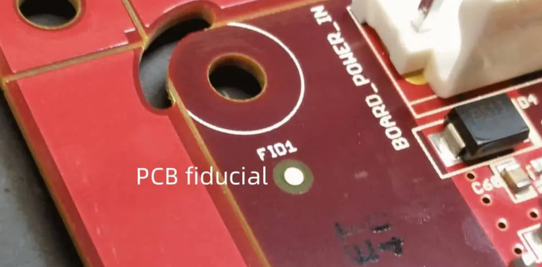
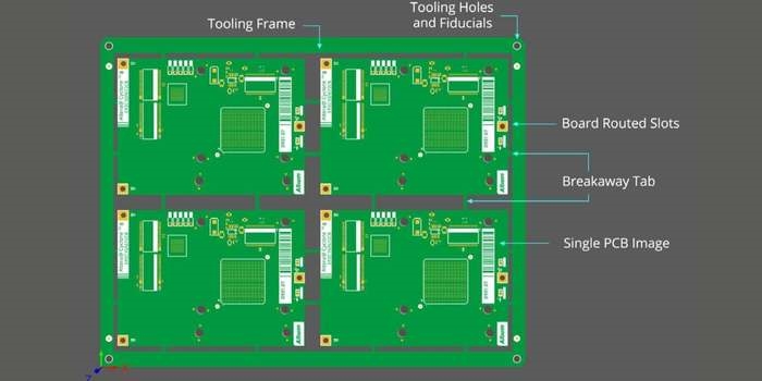
Role of Fiducial Markers
Fiducial markers are small reference points on a PCB used by automated assembly equipment to align the board accurately. In high-density designs, where precision is paramount, fiducial markers play a vital role. These markers should be placed in at least three non-collinear locations on the board to provide a reliable reference for vision systems. Global fiducials help locate the entire board, while local fiducials assist with precise placement of fine-pitch components. Standards such as IPC-6012E recommend clear, unobstructed placement of fiducials away from copper traces or component pads to avoid interference during detection.
Pick and Place Optimization
Automated pick and place systems are integral to assembling high-density PCBs due to their speed and accuracy. DFA considerations for pick and place optimization include designing the board layout to minimize tool head travel distance. This can be achieved by clustering components that share the same feeder or nozzle type. Engineers should also ensure that component data, including centroid coordinates and rotation, is accurately defined in the design files to avoid placement errors. Adhering to standards like IPC-7351B for land pattern design supports compatibility with automated equipment, ensuring precise component mounting.
Practical Solutions and Best Practices for DFA
Minimizing Assembly Steps
Reducing the number of assembly steps is a core DFA principle that directly impacts production efficiency. For high-density PCBs, engineers can minimize steps by standardizing component types and reducing the variety of packages used. For example, using a single capacitor value across multiple locations decreases the need for feeder changes during assembly. Additionally, designing for single-sided assembly, when possible, eliminates the need to flip the board during production, saving time and reducing handling errors. Following guidelines from IPC-A-610G for assembly acceptability ensures that designs are practical for streamlined manufacturing processes.
Component Placement Best Practices
Effective component placement DFA involves strategic planning to balance density with manufacturability. Engineers should place larger components first to anchor the layout, followed by smaller components in the remaining spaces. Critical components, such as high-speed ICs, should be positioned to minimize signal path lengths, while connectors should be near board edges for easy access during testing. Maintaining a grid-based layout for components can also simplify programming for automated equipment. Compliance with IPC-2221B for design standards ensures that placement strategies meet industry expectations for reliability and assembly ease.
Fiducial Marker Implementation
Implementing fiducial markers correctly is essential for high-density PCB assembly. Engineers should use a minimum of three global fiducials, ideally placed at the corners of the board, to provide a stable reference frame. Local fiducials are recommended near fine-pitch components or areas requiring high precision. The markers should be designed as small, circular copper pads without solder mask coverage, ensuring clear visibility for vision systems. Following IPC-6012E specifications for fiducial design helps maintain consistency and compatibility with assembly processes.
Enhancing Pick and Place Efficiency
To optimize pick and place operations, engineers must provide accurate and complete assembly data. This includes detailed bill of materials (BOM) files and precise pick and place files with component coordinates. Designing for minimal nozzle changes by grouping components with similar handling requirements can significantly reduce assembly time. Additionally, ensuring that components are sourced with standard packaging, such as tape and reel, supports seamless integration with automated systems. Adhering to IPC-7351B for footprint design aids in maintaining alignment accuracy during placement.
Design Verification and Testing
Before finalizing a high-density PCB design, thorough verification is necessary to ensure DFA principles are effectively applied. Design rule checks (DRC) should be conducted to validate spacing, orientation, and fiducial placement. Simulation tools can predict potential assembly issues, such as component interference or alignment challenges. Post-assembly testing, aligned with IPC-A-610G standards, helps confirm that the design supports reliable manufacturing. Iterative feedback from assembly teams can also refine future designs for better efficiency.
Conclusion
Design for Assembly is a pivotal approach for ensuring the manufacturability of high-density PCBs. By focusing on strategic component placement, incorporating fiducial markers, optimizing for pick and place systems, and minimizing assembly steps, electrical engineers can significantly enhance production efficiency and product reliability. Adhering to established industry standards, such as those from IPC, provides a robust framework for implementing DFA principles. As PCB designs continue to grow in complexity, integrating these considerations early in the design process remains essential for achieving seamless assembly and high-quality outcomes.
FAQs
Q1: How does component placement DFA improve high-density PCB assembly?
A1: Component placement DFA enhances assembly by organizing components logically, reducing setup changes, and ensuring consistent orientation. Grouping similar components minimizes pick and place tool adjustments, while proper spacing prevents soldering issues. Following industry standards for layout ensures compatibility with automated systems, leading to faster production and fewer errors during the assembly of high-density PCBs.
Q2: Why are fiducial markers critical for high-density PCB designs?
A2: Fiducial markers are vital for precise alignment in high-density PCB assembly. They provide reference points for automated vision systems to locate the board and components accurately. Placing global and local fiducials as per industry guidelines ensures error-free positioning, especially for fine-pitch components, making them indispensable for maintaining accuracy in complex designs.
Q3: What strategies help in minimizing assembly steps for PCBs?
A3: Minimizing assembly steps involves standardizing component types and designing for single-sided assembly when feasible. Using uniform packages reduces feeder changes, while limiting board flips cuts handling time. These strategies streamline the process, lower production costs, and reduce error risks, ensuring efficient assembly for high-density PCBs while adhering to recognized standards.
Q4: How can pick and place optimization impact PCB assembly efficiency?
A4: Pick and place optimization boosts efficiency by reducing tool head travel and nozzle changes through strategic component grouping. Accurate design files with precise coordinates prevent placement errors. Designing for standard packaging compatibility further speeds up the process. This approach ensures faster, more reliable assembly of high-density PCBs with minimal downtime.
References
IPC-6012E — Qualification and Performance Specification for Rigid Printed Boards. IPC, 2020.
IPC-A-600K — Acceptability of Printed Boards. IPC, 2020.
IPC-A-610G — Acceptability of Electronic Assemblies. IPC, 2017.
IPC-7351B — Generic Requirements for Surface Mount Design and Land Pattern Standard. IPC, 2010.
IPC-2221B — Generic Standard on Printed Board Design. IPC, 2012.


