Introduction
In the fast-paced world of electronics, speed to market often defines success. Quick-turn PCB manufacturing addresses this need by accelerating production timelines without compromising quality. However, achieving rapid turnaround times starts with a well-optimized PCB layout. Effective design practices, including precise component placement and adherence to manufacturing rules, can significantly reduce production delays. This article explores essential PCB layout guidelines tailored for quick-turn processes. It covers critical aspects like routing strategies, design rules for manufacturability, and tips to streamline the transition from design to production. Aimed at electrical engineers, these insights ensure designs meet industry standards while minimizing errors and rework. By focusing on practical solutions, this guide helps optimize every stage of the quick-turn PCB design process.
What Is Quick-Turn PCB Design and Why It Matters
Quick-turn PCB design refers to the process of creating printed circuit board layouts optimized for rapid prototyping and manufacturing. Unlike traditional timelines that may span weeks, quick-turn services aim to deliver boards in days or even hours. This approach is vital for industries requiring fast iterations, such as consumer electronics, medical devices, and automotive systems. The ability to test and refine designs swiftly can accelerate product development cycles and provide a competitive edge.
The significance of quick-turn design lies in its alignment with tight project schedules. A poorly prepared layout can lead to manufacturing delays, increased costs, or functional failures. By prioritizing PCB layout guidelines specific to quick-turn needs, engineers ensure designs are manufacturable from the outset. This reduces the risk of revisions and enhances collaboration with fabrication teams, ultimately supporting faster time to market.
Technical Principles of Quick-Turn PCB Layout
Understanding the core principles behind PCB layout for quick-turn manufacturing is essential for success. The primary goal is to create designs that minimize production bottlenecks. This involves adhering to design rules for PCB manufacturing and anticipating common fabrication challenges.
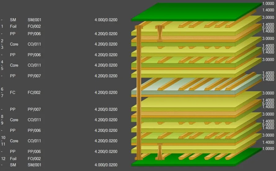
One key principle is design for manufacturability (DFM). DFM focuses on simplifying the production process by aligning the layout with standard fabrication capabilities. For instance, maintaining consistent trace widths and spacing prevents issues during etching or drilling. Another principle is minimizing complexity in layer stackups. While multilayer boards offer design flexibility, excessive layers can slow down manufacturing due to added processing steps.
Signal integrity also plays a critical role. In quick-turn scenarios, there is little time for extensive testing or redesign. Ensuring proper impedance control and avoiding crosstalk during the initial layout phase helps maintain performance. These principles, rooted in industry standards like IPC-2221B, form the foundation for efficient quick-turn PCB design.
Essential PCB Layout Guidelines for Speedy Manufacturing
To achieve rapid turnaround times, engineers must follow specific PCB layout guidelines tailored for quick-turn processes. These best practices address common manufacturing constraints and ensure smooth production.
Optimize Component Placement
Component placement is a cornerstone of effective PCB design. Strategic positioning reduces routing complexity and enhances assembly efficiency. Place critical components, such as microcontrollers or high-speed connectors, first to define primary signal paths. Group related components together to shorten trace lengths and minimize interference. Ensure adequate spacing between components to avoid thermal or mechanical issues during assembly, adhering to guidelines in IPC-7351B for surface mount land patterns.
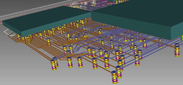
Streamline PCB Routing
Efficient PCB routing directly impacts manufacturing speed. Prioritize direct, short traces to reduce signal delays and simplify fabrication. Avoid unnecessary vias, as they increase drilling time and potential defects. Route high-speed signals on inner layers when possible to shield them from external noise. Maintain consistent trace widths and spacing as per IPC-2221B to prevent etching inconsistencies. Automated routing tools can assist, but manual review ensures critical paths meet design intent.
Adhere to Design Rules for PCB Manufacturing
Design rules for PCB manufacturing are non-negotiable in quick-turn environments. These rules cover minimum trace widths, clearances, and hole sizes based on fabrication capabilities. For instance, maintaining a minimum annular ring around vias ensures reliable drilling, as specified in IPC-6012E. Avoid tight tolerances unless absolutely necessary, as they can delay production. Always validate designs against manufacturer-provided DFM checklists to catch issues early.
Simplify Board Outline and Features
Complex board shapes or excessive cutouts can slow down manufacturing. Stick to standard rectangular outlines unless the application demands otherwise. Limit internal slots or non-standard features, as they require additional tooling. Clear edge clearances, as recommended by IPC-A-600K, prevent damage during panelization and depanelization processes.
Suggested Reading: From Prototype to Production: Scaling with Quick Turn PCB Manufacturing
Best Practices for Quick-Turn PCB Design
Beyond basic guidelines, adopting best practices elevates the quick-turn design process. These actionable tips focus on collaboration, preparation, and error prevention.
Communicate Early with Fabrication Teams
Engage with manufacturing partners during the design phase. Share preliminary layouts to confirm compliance with their equipment capabilities. Discuss stackup options, material availability, and any quick-turn constraints. Early feedback helps avoid last-minute redesigns and aligns expectations for turnaround times.
Use Standard Materials and Processes
Opt for widely available materials and standard manufacturing processes. Non-standard laminates or finishes, while sometimes necessary, often extend lead times due to sourcing delays. Stick to common copper weights and dielectric thicknesses as outlined in IPC-4101E to ensure immediate availability. Standard surface finishes also simplify assembly preparation.
Perform Thorough Design Reviews
Before submission, conduct comprehensive design rule checks (DRC) and electrical rule checks (ERC). These validations catch errors like unconnected nets or clearance violations. Simulate signal integrity for high-speed designs to preempt performance issues. A clean design file, free of errors, speeds up the manufacturer’s review process.
Prepare Complete Documentation
Incomplete documentation is a frequent cause of delays in quick turn PCB fabrication. Provide clear Gerber files, drill files, and a bill of materials (BOM). Include fabrication notes specifying layer stackup, tolerances, and testing requirements. Reference standards like IPC-A-610G for assembly criteria to ensure clarity. Well-organized files reduce back-and-forth communication and expedite production.

Common Challenges in Quick-Turn PCB Design and Solutions
Quick-turn PCB design often presents unique challenges due to compressed timelines. Addressing these issues proactively ensures deadlines are met without sacrificing quality.
One common challenge is incomplete design validation. Rushing the process may overlook critical errors, leading to failed prototypes. The solution is to integrate automated DRC tools early and allocate time for manual inspection. Another issue is component availability. Last-minute shortages can halt assembly. Cross-reference the BOM with supplier inventories during design to confirm stock levels.
Tight schedules can also strain communication with manufacturers. Misaligned expectations on capabilities or timelines cause delays. Establish a direct line of contact and confirm key details like panel sizes or testing protocols upfront. Finally, high-speed designs may suffer from signal integrity issues if not carefully planned. Follow guidelines from IPC-2141A for controlled impedance to mitigate risks.
Conclusion
Quick-turn PCB manufacturing offers a powerful solution for accelerating product development in competitive industries. However, success hinges on meticulous PCB layout guidelines and adherence to design rules for PCB manufacturing. Strategic component placement, streamlined routing, and early collaboration with fabrication teams are vital to minimizing delays. By incorporating best practices like thorough design reviews and complete documentation, engineers can ensure rapid turnaround without compromising reliability. Aligning designs with industry standards further enhances manufacturability and performance. With these essential tips, quick-turn PCB design becomes a seamless process, enabling faster iterations and quicker paths to market for innovative electronic solutions.
FAQs
Q1: How does component placement affect quick-turn PCB design?
A1: Component placement is critical in quick-turn PCB design as it influences routing efficiency and assembly speed. Positioning related components closely reduces trace lengths, minimizing signal delays and interference. Proper spacing also prevents thermal issues during soldering, ensuring faster production. Following standards like IPC-7351B for land patterns helps achieve optimal placement for rapid manufacturing.
Q2: What are key PCB layout guidelines for speedy manufacturing?
A2: Key PCB layout guidelines include maintaining consistent trace widths, ensuring proper clearances, and simplifying board outlines. Adhering to design rules for PCB manufacturing, such as those in IPC-6012E, avoids fabrication errors. Using standard materials and minimizing vias or complex features further accelerates the process by aligning with common production capabilities.
Q3: Why is PCB routing important for quick-turn projects?
A3: PCB routing directly impacts manufacturing speed and signal integrity in quick-turn projects. Short, direct traces reduce fabrication time and signal delays. Avoiding excessive vias minimizes drilling steps, while following IPC-2221B for spacing prevents etching issues. Efficient routing ensures designs are production-ready, cutting down on rework and delays.
Q4: How can design rules for PCB manufacturing reduce turnaround time?
A4: Design rules for PCB manufacturing, like those in IPC-A-600K, set minimum standards for traces, holes, and clearances. Adhering to these rules prevents production errors, reducing the need for revisions. Consistent alignment with fabrication capabilities ensures smooth processing, minimizing delays and enabling faster delivery in quick-turn scenarios.
References
IPC-2221B — Generic Standard on Printed Board Design. IPC, 2012.
IPC-7351B — Generic Requirements for Surface Mount Design and Land Pattern Standard. IPC, 2010.
IPC-6012E — Qualification and Performance Specification for Rigid Printed Boards. IPC, 2020.
IPC-A-600K — Acceptability of Printed Boards. IPC, 2020.
IPC-4101E — Specification for Base Materials for Rigid and Multilayer Printed Boards. IPC, 2017.
IPC-A-610G — Acceptability of Electronic Assemblies. IPC, 2017.
IPC-2141A — Design Guide for High-Speed Controlled Impedance Circuit Boards. IPC, 2004.


