Introduction
In-circuit testing stands as a critical step in printed circuit board assembly to verify functionality and detect defects before final deployment. This process targets assembled boards by measuring electrical characteristics of components and interconnections, ensuring compliance with design intent. Among the primary methods, bed-of-nails testers and flying probe testers dominate due to their effectiveness in achieving comprehensive defect coverage. Bed-of-nails testers rely on fixed probe arrays for rapid, parallel access to test points, while flying probe testers use movable probes for flexible testing without custom fixtures. Selecting the right approach depends on specific production needs regarding volume scale and design complexity, balancing speed, cost, and adaptability. Factory operations prioritize these testers to minimize escapes and uphold quality standards in high-stakes electronics manufacturing.
Engineers face challenges like shrinking component pitches and increasing board densities, making test coverage essential for reliability. Defects such as opens, shorts, wrong-value components, and solder joint issues can propagate if undetected, leading to field failures. In-circuit testing addresses these by isolating and stimulating circuits under controlled conditions. Both tester types support vectorless and guided probing techniques to maximize fault detection. As production scales vary from prototypes to mass runs, understanding approach and application suitability guides optimal implementation.
What Is In-Circuit Testing and Why It Matters
In-circuit testing involves placing a fully or partially assembled printed circuit board into a tester that applies stimuli to nets and components, then compares responses against expected values. This method verifies passive components like resistors and capacitors, checks active devices such as diodes and transistors, and confirms interconnections for continuity and isolation. Unlike functional testing, which evaluates the entire board as a system, in-circuit testing focuses on individual elements to pinpoint manufacturing defects early in the process. Factory-driven insights emphasize its role in reducing rework costs and improving yield rates.
The relevance stems from its ability to achieve high fault coverage, often exceeding 90 percent for accessible points, depending on test program sophistication. In high-reliability sectors, undetected defects compromise system performance, violating standards like IPC-A-610 for acceptability of electronic assemblies. Production teams integrate in-circuit testing post-surface mount technology placement and reflow soldering to catch assembly anomalies before final assembly. This proactive approach aligns with quality management systems outlined in ISO 9001, ensuring consistent defect detection across batches.
Design complexity influences test point accessibility, with double-sided boards or fine-pitch ball grid arrays requiring precise probe placement. Volume scale dictates economic viability, as high-throughput environments demand fast cycle times. Engineers benefit from data analytics generated by these testers, informing process improvements and supplier feedback loops. Ultimately, in-circuit testing bridges design verification and production reality, safeguarding end-product integrity.
Technical Principles of Bed-of-Nails Testers
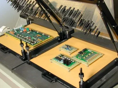
Bed-of-nails testers employ a custom-machined fixture embedding hundreds or thousands of spring-loaded probes arranged to contact designated test points on the board underside. When the fixture presses the PCB into position, all probes engage simultaneously, enabling parallel electrical measurements across multiple nodes. The system injects analog or digital signals to perform parametric tests on components and digital vectors for logic states, detecting discrepancies like out-of-tolerance values or stuck faults. Mechanical alignment ensures repeatability, with probe spacing typically accommodating 0.1-inch grids but adaptable to denser layouts via custom tooling.
This parallel architecture yields test times under 60 seconds per board, ideal for high-volume runs where throughput trumps flexibility. Limitations arise with board warpage or tall components interfering with fixture contact, necessitating mechanical clamping or vacuum hold-downs. Test programs incorporate guard bands to isolate nets from adjacent influences, enhancing measurement accuracy amid densely packed circuits. Factory protocols calibrate probes regularly to maintain low contact resistance, typically below 5 ohms.
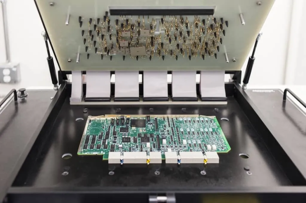
Development of the fixture demands upfront investment, including CAD data translation and mechanical prototyping, often taking weeks for complex boards. Once built, it supports unlimited testing without reprogramming for identical designs, amortizing costs over large volumes. Integration with automated handlers boosts efficiency in inline production lines. Engineers appreciate the high node count access, facilitating comprehensive shorts and opens testing across the entire board.
Technical Principles of Flying Probe Testers
Flying probe testers feature a small number of independently controlled probes, usually four to eight, mounted on robotic arms that move precisely over the board surface. Software directs probes to sequential test points via XY gantries, contacting pads or vias with minimal force to avoid damage. This fixtureless method relies on laser-guided positioning for accuracies down to 10 microns, enabling tests on fine-pitch components inaccessible to fixed beds. Parametric measurements and boundary scans proceed node-by-node, building a fault dictionary through pattern recognition.
Test speeds range from 2 to 10 seconds per net, slower than bed-of-nails but sufficient for low-volume scenarios due to no fixture delays. Multi-probe configurations allow simultaneous actions, like one probing while others measure, optimizing cycle times. Vision systems assist in fiducial alignment and component presence checks, compensating for board tolerances. Factory versatility shines in handling irregular shapes or multi-sided boards by flipping or rotating automatically.
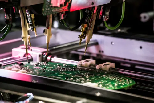
Programming occurs directly from netlist or Gerber files, with changes implemented in hours rather than weeks. This agility suits prototypes and frequent revisions, where design iterations outpace production stability. Advanced models incorporate high-voltage probing for power integrity and environmental chambers for stressed testing. Coverage extends to backside access without fixtures, broadening defect detection capabilities.
Approach and Application Suitability
Approach and application suitability hinges on balancing test speed, cost, flexibility, and fault coverage against specific production needs regarding volume scale and design complexity. Bed-of-nails testers excel in high-volume manufacturing, where fixture costs distribute over thousands of units, delivering sub-minute cycle times for stable designs. Their parallel probing maximizes throughput, suiting automotive or consumer electronics lines with consistent revisions. However, high design complexity, such as high-density interconnects or odd-form boards, inflates fixture expenses and risks probe damage from tight pitches.
Flying probe testers align with low to medium volumes, prototypes, and complex designs, eliminating fixture investments and enabling rapid setup for new products. They navigate intricate layouts with ease, accessing test points under components or on inner layers via double-sided probing. For volume scales below 1,000 units, their per-board economics surpass bed-of-nails, especially amid design changes. Drawbacks include longer test times, potentially bottlenecking if scaled inappropriately.
- Volume Scale: Bed-of-nails — High (10,000+ units); Flying probe — Low-Medium (<5,000 units)
- Design Complexity: Bed-of-nails — Low-Medium (standard pitches); Flying probe — High (fine-pitch, HDI)
- Upfront Cost: Bed-of-nails — High (fixture); Flying probe — Low (fixtureless)
- Test Speed: Bed-of-nails — Fast (parallel); Flying probe — Slower (sequential)
- Flexibility: Bed-of-nails — Low (design-specific); Flying probe — High (programmable)
Hybrid strategies emerge for mixed needs, starting with flying probes for NPI then transitioning to bed-of-nails for ramp-up. J-STD-001 requirements for soldered assemblies guide test limits, ensuring measurements reflect assembly quality. Procurement teams evaluate total cost of ownership, factoring yield impacts from test escapes.
Best Practices for Complete Defects Coverage
Achieve complete defects coverage by optimizing test point allocation during design, targeting 80-95 percent node access while adhering to IPC-6012 performance specifications. Allocate test points at component leads, vias, and nets prone to faults, spacing them at least 0.05 inches apart to prevent crosstalk. Develop test programs with boundary scan integration for inaccessible areas, combining vectorless techniques like capacitance mapping for opens and shorts. Factory best practices include pre-test continuity checks on fixtures and statistical process control on measurements to flag drifts.
Calibrate systems per manufacturer guidelines, verifying probe integrity and analog accuracy before runs. For bed-of-nails, employ progressive fixturing with adjustable pressures to handle warpage compliant with IPC standards. Flying probe users leverage auto-learn features to refine probe paths, minimizing wear on high-speed axes. Combine in-circuit with automated optical inspection upstream for synergistic coverage, reducing false calls.
Troubleshoot systematically by segmenting tests into power-up, analog, and digital phases, isolating failures via fault grading software. Document thresholds aligned with component tolerances, avoiding over-specification that inflates rejects. Regular audits against ISO 9001 ensure process repeatability. These practices maximize yield while containing costs across volume scales.
Conclusion
Different in-circuit testing methods, particularly bed-of-nails testers and flying probe testers, provide tailored solutions for complete defects coverage based on production realities. High-volume operations leverage bed-of-nails for speed and economy, while complex, low-scale runs favor flying probes for versatility. Approach and application suitability demands evaluating volume scale and design complexity alongside total ownership costs. Integrating standards like IPC-A-610, J-STD-001, and IPC-6012 ensures factory-grade reliability. Engineers achieve optimal outcomes by aligning tester choice with workflow, enhancing quality from prototype to production.
FAQs
Q1: What are the main differences between bed-of-nails testers and flying probe testers in terms of approach and application suitability?
A1: Bed-of-nails testers use fixed parallel probes for high-speed testing suited to large volume scale and simpler designs, offering fast cycle times after fixture investment. Flying probe testers employ movable probes for sequential access, ideal for low-volume and high design complexity with no fixtures needed. Selection depends on balancing throughput needs against flexibility, ensuring defect coverage without production bottlenecks. Factory insights prioritize bed-of-nails for stable high-runs and flying probes for prototypes.
Q2: When should electric engineers choose bed-of-nails testers for specific production needs regarding volume scale?
A2: Opt for bed-of-nails testers in high-volume scenarios exceeding thousands of units, where parallel probing amortizes fixture costs and delivers rapid throughput. They suit standardized designs with ample test point access, aligning with IPC standards for assembly verification. Avoid for low volumes due to high upfront expenses. This choice maximizes efficiency in mass production lines.
Q3: How do flying probe testers handle design complexity compared to bed-of-nails testers?
A3: Flying probe testers excel in complex designs with fine pitches and irregular layouts, using precise robotics for accessible probing without custom tooling. They adapt quickly to changes, supporting prototypes and medium volumes. Bed-of-nails struggle with density due to fixture limitations. Engineers gain comprehensive coverage for high-complexity boards through programmable paths.
Q4: Can combining bed-of-nails and flying probe testers improve defects coverage?
A4: Yes, hybrid use starts with flying probes for low-volume validation then shifts to bed-of-nails for scaled production, covering diverse needs. This ensures early defect detection transitioning to high throughput. Standards like J-STD-001 guide consistent criteria. Factories implement based on volume scale and complexity for optimal results.
References
IPC-A-610H — Acceptability of Electronic Assemblies. IPC, 2019
IPC-6012E — Qualification and Performance Specification for Rigid Printed Boards. IPC, 2017
J-STD-001G — Requirements for Soldered Electrical and Electronic Assemblies. IPC, 2017
ISO 9001:2015 — Quality Management Systems. ISO, 2015


