Introduction
Drill holes form the backbone of interconnects in printed circuit boards, enabling vias, component mounting, and mechanical fixtures. In design for manufacturability (DFM), overlooking drill hole parameters leads to frequent production delays, yield losses, and reliability failures. Electric engineers must prioritize PCB drill size DFM, drill-to-copper clearance, aspect ratio drill holes, plated through hole DFM, and non-plated through hole DFM to streamline fabrication. Factory experience shows that proactive DFM checks catch issues early, reducing scrap rates from drilling inaccuracies or plating defects. This article explores these considerations through a manufacturing lens, drawing on standard-aligned practices to guide robust designs. By understanding common pitfalls, engineers can deliver boards that meet performance demands without costly revisions.

What Are Drill Hole Considerations in PCB DFM and Why Do They Matter?
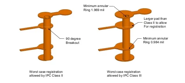
Drill hole considerations in PCB DFM encompass the selection of hole diameters, positional tolerances, and interactions with surrounding features to ensure repeatable fabrication. These factors directly influence drilling precision, plating uniformity, and overall board integrity. In high-volume production, deviations in PCB drill size DFM cause misalignment during assembly or weakened structures under thermal stress. Manufacturers evaluate designs against capabilities like drill bit availability and machine accuracy, where non-standard sizes inflate tooling costs and cycle times. Aspect ratio drill holes play a pivotal role, as excessive ratios strain plating processes and compromise void-free fills. Ultimately, adhering to these principles aligns design intent with factory realities, minimizing defects like breakout or smear that trigger rework.
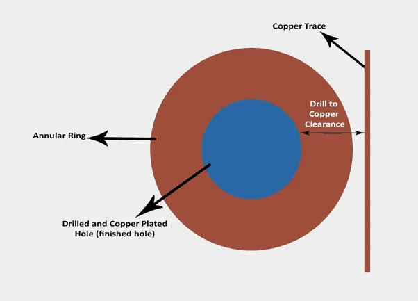
From a factory perspective, drill-to-copper clearance emerges as a critical metric to prevent shorts during mechanical or laser drilling. Inadequate spacing allows drill wander to nick adjacent traces, especially in dense multilayer stacks. Plated through hole DFM demands extra attention to plating buildup, which narrows finished holes and alters electrical performance. Non-plated through hole DFM focuses more on mechanical tolerances for fiducials or edge connectors. Neglecting these invites reliability issues in field use, such as intermittent connections from plating cracks. Standards like IPC-6012E provide benchmarks for hole quality, ensuring boards withstand environmental stresses.
Key Technical Principles Behind Drill Hole DFM
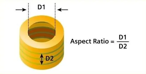
The aspect ratio for drill holes, defined as board thickness divided by finished hole diameter, governs plating chemistry flow and copper deposition uniformity. High aspect ratios restrict electrolyte penetration, fostering voids or thin plating at hole bottoms that fail under current stress. Factories mitigate this by recommending balanced stackups where drill diameters scale with layer count. Mechanical drilling introduces smear from resin displacement, necessitating desmear processes to expose inner layers cleanly. Laser drilling for microvias offers finer control but amplifies aspect ratio sensitivities due to tapered profiles.
Drill-to-copper clearance accounts for drill bit deflection, breakout tendencies, and post-plating dimensions. During entry and exit, bits can veer by tolerances tied to material hardness and speed settings, eroding nearby copper if spacing is tight. In multilayer boards, inner layer alignment hinges on this clearance to avoid interlayer shorts post-lamination. Plating adds annular buildup, effectively reducing clearance further, which demands upfront compensation in design files. Factories simulate these interactions to flag risks, emphasizing symmetric hole patterns for stable drilling.
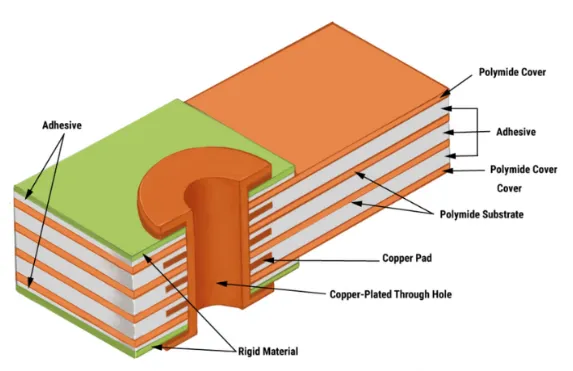
Plated through holes (PTH) integrate electroless and electrolytic copper to form conductive barrels, where drill size influences wall thickness control. Oversized drills dilute plating efficiency, while undersized ones overload chemistry with debris. Non-plated through holes (NPTH) skip plating, prioritizing clean walls for press-fit pins or screws, but still require anti-drill-break tabs in panels. Both types benefit from standard drill charts that align with bit inventories, reducing setup times. IPC-A-600K outlines acceptability criteria for hole geometry, guiding inspections for roughness or oversize.
Practical Best Practices for Drill Hole DFM
Start with standard drill sizes from fabrication drawings to leverage pre-tooled bits, optimizing throughput in production runs. Custom sizes demand verification against machine limits, often extending lead times. For PCB drill size DFM, cluster holes by diameter to minimize tool changes, and specify tolerances per IPC class—typically tighter for high-reliability boards. Incorporate drill breakouts or routing for edge holes to contain debris and protect panels.
Maintain generous drill-to-copper clearance, factoring in plating thickness and drill wander—aim for margins that accommodate process variations without sacrificing density. Simulate clearances in design software against stackup data, consulting fabricator DFM reports early. Aspect ratio drill holes should prioritize larger diameters for thicker boards, distributing vias evenly to avoid localized stress during lamination. Factories prefer aspect ratios that support uniform resin flow, preventing warpage around dense via fields.
Differentiate plated through hole DFM by specifying finished hole sizes post-plating, allowing for buildup on walls and annuli. Use panelization with breakaway tabs for NPTH mounting holes to simplify depaneling without burrs. Implement sequential lamination for high-aspect designs, drilling incrementally to control tolerances. Always generate separate drill files for PTH and NPTH, including netlist associations for automated checks. Post-DFM reviews confirm compliance, catching oversights like unbalanced copper that skew drill accuracy.
Common Manufacturing Errors and Troubleshooting Insights
A prevalent error in PCB drill size DFM is selecting non-standard diameters, leading to drill breakage or prolonged setups. Engineers troubleshoot by reviewing drill charts and opting for increments like 0.05 mm steps. Insufficient drill-to-copper clearance manifests as copper smearing into holes, detectable via cross-section analysis. Factories recommend increasing spacing or rerouting traces during respins.
High aspect ratio drill holes trigger plating voids, evident in reliability tests as high-resistance vias. Mitigation involves downsizing board thickness or upsizing holes, balanced against signal integrity. Plated through hole DFM pitfalls include excessive plating roughness from poor desmear, addressed by plasma etching enhancements. Non-plated through hole DFM errors like oversize from drill wander affect mechanical fits—use fixtures for precision drilling.
Factory data highlights symmetric hole placement reduces Z-axis misalignment in multilayers. Troubleshooting erratic hole sizes points to peck drilling needs for deep holes, clearing chips iteratively. Integrating these fixes up front prevents escalation to full-panel rejects.
Conclusion
Mastering drill hole considerations in PCB DFM safeguards against manufacturing hurdles, ensuring high yields and reliable boards. Key focus areas—PCB drill size DFM, drill-to-copper clearance, aspect ratio drill holes, plated through hole DFM, and non-plated through hole DFM—demand factory-informed decisions. By embedding standard practices like those in IPC-2221, engineers bridge design and production seamlessly. Proactive checks yield cost savings and faster time-to-market. Prioritize these elements for designs that perform under real-world conditions, from prototypes to volume runs.
FAQs
Q1: What is the importance of drill-to-copper clearance in PCB DFM?
A1: Drill-to-copper clearance prevents drill bit breakout into adjacent traces during fabrication, avoiding shorts in multilayer boards. Factories require sufficient spacing to account for bit deflection and plating buildup, ensuring clean inner layer exposure. Inadequate clearance leads to yield losses, making it a cornerstone of robust DFM checklists for electric engineers.
Q2: How does aspect ratio affect drill holes in PCB manufacturing?
A2: Aspect ratio, board thickness over hole diameter, influences plating uniformity and void formation in PTH. High ratios hinder electrolyte flow, compromising reliability under thermal cycling. Manufacturers align designs to practical limits for consistent results, integrating this into stackup planning for optimal DFM.
Q3: What distinguishes plated through hole DFM from non-plated through hole DFM?
A3: Plated through hole DFM incorporates plating tolerances and wall thickness control for conductivity, demanding precise drill sizes to avoid narrowing. Non-plated through hole DFM emphasizes mechanical accuracy for fits, with looser specs but similar clearance needs. Both require distinct files to streamline production workflows.
Q4: Why prioritize PCB drill size DFM in early design stages?
A4: PCB drill size DFM ensures compatibility with standard tooling, minimizing custom setups and delays. Selecting from approved charts matches fabricator capabilities, reducing breakage risks. Early adherence prevents respins, aligning with standards for high-volume efficiency.
References
IPC-2221 — Generic Standard on Printed Board Design. IPC
IPC-6012E — Qualification and Performance Specification for Rigid Printed Boards. IPC, 2017
IPC-A-600K — Acceptability of Printed Boards. IPC, 2020