What Are IPC Standards for ENIG, and Why Are They Important?
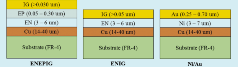
IPC standards represent globally recognized guidelines developed by the Institute of Printed Circuits (now simply known as IPC) to guarantee quality, reliability, and uniformity in electronics manufacturing. For Electroless Nickel Immersion Gold (ENIG), a widely adopted surface finish in PCB production, the principal guiding document is IPC-4552. This specification meticulously outlines the requirements for both electroless nickel and immersion gold plating, ensuring the finish can withstand subsequent soldering processes and various environmental stresses.
Adhering to ENIG IPC standards is paramount for several critical reasons. Firstly, it provides assurance that the PCB finish will perform reliably during the assembly phase and throughout the lifespan of the final product. Secondly, compliance with IPC-4552 actively helps manufacturers prevent common issues such as nickel corrosion or the infamous "black pad" defects, both of which can lead to catastrophic solder joint failures. Lastly, consistently meeting these standards fosters trust with clients, clearly demonstrating a steadfast commitment to quality. The following sections will delve into the specifics of ENIG IPC 4552, detailing plating quality benchmarks, thickness specifications, and practical advice for maintaining compliance throughout your manufacturing operations.
Deciphering ENIG IPC 4552: The Benchmark for Finish Quality
The IPC-4552 standard, initially introduced in 2002, has undergone various revisions, such as IPC-4552B, to keep pace with evolving challenges in modern PCB manufacturing. This standard specifically addresses the requirements for ENIG plating, with a strong focus on the precise thickness of the nickel and gold layers, resistance to corrosion, and overall performance under diverse operational conditions.
A significant enhancement in IPC-4552B, a recent revision, is its heightened emphasis on preventing nickel corrosion. While earlier versions primarily focused on thickness, the latest update offers comprehensive guidelines for assessing and mitigating corrosion risks. This is critically important because excessive corrosion can compromise the structural integrity of the nickel layer, leading to poor solderability and potential failures in demanding applications, such as those found in aerospace or medical devices. The standard also provides a structured framework for manufacturers to rigorously test and validate their ENIG processes. By diligently following IPC-4552, suppliers can ensure their surface finishes are robust enough to perform reliably across diverse manufacturing environments and consistently meet customer expectations.
Key Requirements of ENIG IPC 4552
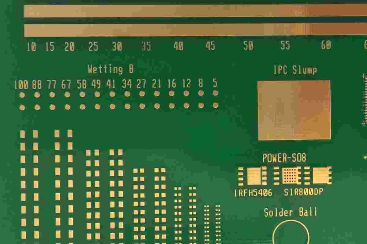
● Nickel Layer Thickness: Typically mandated to be between 3 to 6 micrometers (µm). This thickness is crucial for forming a robust barrier against corrosion and ensuring the durability required during the soldering process.
● Gold Layer Thickness: Recommended to range from 0.05 to 0.1 µm. The gold layer must be sufficiently thin to manage costs but adequate enough to protect the underlying nickel. IPC guidelines caution that gold thickness exceeding 0.125 µm can elevate the risk of nickel corrosion due to inherent process variability.
● Corrosion Resistance: The finished surface must exhibit resilience against degradation when subjected to thermal and environmental stresses, thereby guaranteeing long-term reliability.
● Solderability: The ENIG finish must consistently facilitate the formation of strong, reliable solder joints, even after enduring multiple reflow cycles, particularly during lead-free soldering processes.
By strictly adhering to these precise specifications, manufacturers can produce ENIG finishes that strike an optimal balance between cost-effectiveness, performance, and unwavering reliability.
Ensuring High ENIG Plating Quality: What Manufacturers Need to Know
The quality of ENIG plating directly influences a PCB’s overall performance and its operational lifespan. Substandard plating can lead to severe defects, notably the "black pad" phenomenon, where nickel corrosion impedes proper soldering, resulting in compromised or failed connections. To consistently achieve high ENIG plating quality, manufacturers must prioritize stringent process control, careful material selection, and continuous, rigorous testing.
Critical Factors Influencing ENIG Plating Quality
Process Consistency is paramount; both the electroless nickel and immersion gold deposition processes require exceptionally tight control, particularly for high-frequency PCB applications where surface finish uniformity directly impacts signal integrity. Even minor fluctuations in bath chemistry, temperature, or immersion duration can lead to uneven plating or the introduction of defects that may increase insertion loss or impedance variation. Material Purity is another non-negotiable factor; using high-purity chemicals for nickel and gold deposition is fundamental to preventing contamination that could critically compromise the finish. Corrosion Prevention, as strongly emphasized in IPC-4552B, is essential and becomes even more critical for high-frequency PCB designs. This often entails meticulously optimizing the gold deposition process to minimize porosity, which, if present, could expose the nickel layer to detrimental oxidation. Finally, Testing and Validation through regular procedures—such as X-ray fluorescence (XRF) for precise thickness measurements and comprehensive solderability tests—are indispensable for verifying that the plating consistently meets IPC standards.
High-quality ENIG plating not only markedly improves solderability but also significantly enhances the PCB’s resilience in harsh operating environments, making it an ideal choice for demanding applications in the automotive, industrial, and high-end consumer electronics sectors.
ENIG Thickness Specifications: Achieving Optimal Balance
Meeting the precise thickness specifications outlined in IPC-4552 is one of the most critical aspects of ENIG compliance. The thickness of both the nickel and gold layers plays a pivotal role in determining the finish's overall performance and reliability.
Nickel and Gold Thickness Requirements
The nickel layer serves as a vital barrier, situated between the copper substrate and the gold layer, effectively preventing diffusion and corrosion. IPC-4552 recommends a nickel thickness ranging from 3 to 6 µm for the majority of applications. A thickness below 3 µm typically fails to provide adequate protection, whereas exceeding 6 µm generally escalates costs without yielding significant additional performance benefits. For applications demanding high reliability, manufacturers might aim for the upper end of this specified range to ensure maximum durability.
The gold layer, although considerably thinner, holds equal importance. IPC-4552 specifies a gold thickness between 0.05 to 0.1 µm. This range is designed to optimally protect the nickel from oxidation while simultaneously maintaining cost-effectiveness. However, surpassing a thickness of 0.125 µm can introduce risks, as excessive gold deposition might paradoxically instigate nickel corrosion due to inconsistencies in the process. Consequently, manufacturers must meticulously calibrate their immersion gold processes to operate precisely within this narrow window.
Striking the right balance between these two layer thicknesses is absolutely essential for achieving an ENIG finish that effectively meets both stringent performance criteria and economic objectives. Advanced analytical instruments, such as XRF, are frequently employed during production to verify consistent compliance with these crucial specifications.
Ensuring ENIG Compliance in PCB Manufacturing
Achieving consistent ENIG compliance with IPC standards demands a synergistic combination of robust operational processes, highly skilled personnel, and rigorous quality control measures. The following actionable steps outline how manufacturers can ensure their ENIG finishes consistently meet or exceed IPC-4552 requirements.
Strategies for Consistent Compliance
1. Implement Strict Process Controls: Maintain vigilant control over plating bath chemistry, temperature, and immersion durations. Integrating automated systems can facilitate real-time monitoring of these parameters, significantly minimizing the potential for human error and ensuring uniform plating across all production batches.
2. Conduct Regular Testing: Utilize non-destructive testing methodologies, such as XRF, to accurately measure layer thicknesses and confirm they align with IPC-4552 specifications. Additionally, perform comprehensive solderability and corrosion resistance tests to validate the finish's performance under simulated real-world conditions.
3. Train Personnel Thoroughly: Ensure that all staff involved in the ENIG plating process are comprehensively trained in IPC standards and established best practices. A deep understanding of potential defects, such as black pad syndrome, and proactive prevention strategies is fundamental for upholding consistent quality.
4. Partner with Reliable Suppliers: Forge alliances with trusted suppliers for all plating chemicals and raw materials. High-quality inputs form the bedrock of a compliant ENIG finish; substandard materials can lead to expensive rework or critical product failures.
5. Stay Updated on Revisions: IPC standards are dynamic and evolve continuously to address new challenges within electronics manufacturing. Regularly keep abreast of all updates to IPC-4552, including the latest revisions like IPC-4552B, to guarantee your processes remain fully compliant with current industry guidelines.
By systematically implementing these steps, manufacturers can consistently produce ENIG-finished PCBs that not only meet stringent industry standards but also consistently exceed customer expectations.
Benefits of Adhering to ENIG IPC Standards
Compliance with ENIG IPC standards offers a multitude of advantages for both PCB manufacturers and the end-users of their electronic products. Here are some of the most significant benefits:
Advantages of IPC Compliance
● Enhanced Reliability: Types of PCBs featuring compliant ENIG finishes are inherently less susceptible to failure, even when deployed in demanding applications such as automotive systems or medical devices, where reliability is paramount.
● Improved Solderability: Properly executed ENIG plating ensures the formation of robust, highly reliable solder joints, which significantly reduces the incidence of defects during the assembly process.
● Cost Efficiency: By proactively preventing defects and minimizing the need for costly rework, manufacturers can realize substantial savings on production expenditures, enabling them to maintain competitive pricing in the market.
● Customer Trust: A demonstrable adherence to widely recognized standards like IPC-4552 signals a deep commitment to quality, thereby cultivating stronger confidence among clients and strategic partners.
Ultimately, compliance with ENIG IPC standards transcends mere regulatory fulfillment; it represents a crucial strategic advantage within the fiercely competitive PCB manufacturing industry.
Addressing Challenges in Meeting ENIG IPC Standards
While the benefits of compliance are unequivocally clear, achieving consistent adherence to ENIG IPC standards can present notable challenges. Below are some common issues encountered and practical solutions for overcoming them.
Common Challenges and Solutions
Challenge 1: Nickel Corrosion (Black Pad)
Nickel corrosion, frequently manifesting as "black pad," is a notorious problem in ENIG plating. This occurs when the gold layer fails to adequately protect the underlying nickel, leading to oxidation and subsequent poor solderability.
● Solution: Optimize the immersion gold deposition process to minimize porosity and ensure thorough, uniform coverage. Consistent bath maintenance and vigilant monitoring are also crucial in preventing contamination that contributes to corrosion.
Challenge 2: Thickness Variability
Inconsistent plating thicknesses can lead to non-compliance with IPC-4552 specifications, negatively impacting both the performance and the cost-efficiency of the PCB.
● Solution: Implement automated plating systems for precise control over deposition rates and employ advanced measurement tools, such as XRF, for real-time thickness monitoring and immediate adjustments.
Challenge 3: Adapting to Lead-Free Soldering
Lead-free soldering processes, which often necessitate higher temperatures, can exert significant thermal stress on ENIG finishes, exposing any underlying weaknesses in plating quality.
● Solution: Conduct thorough testing of ENIG finishes under simulated lead-free soldering conditions to verify their ability to withstand elevated thermal stress without degrading or compromising performance.
By proactively identifying and addressing these challenges, manufacturers can consistently uphold high standards of quality and maintain robust compliance within their ENIG processes.
Conclusion: Prioritizing Quality Through ENIG IPC Standards
In the dynamic and competitive landscape of PCB manufacturing, strict adherence to ENIG IPC standards, particularly IPC-4552, is indispensable for ensuring the unwavering quality, reliability, and ultimate customer satisfaction. By maintaining a sharp focus on plating quality, consistently meeting specified thickness requirements, and deploying robust compliance strategies, manufacturers are empowered to produce ENIG-finished PCBs that not only perform exceptionally but also exhibit superior durability. Whether your design objectives cater to mainstream consumer electronics or critical high-reliability applications, a profound understanding and diligent application of these standards will undoubtedly position you at the forefront of the industry.


