What Are Solder Joint Voids and Why Are They a Concern?
Solder joint voids are essentially empty pockets or air bubbles trapped within the metallic connection that fastens an electronic component to a printed circuit board. These imperfections can critically undermine the integrity of the joint, leading to a host of problems. They diminish the mechanical strength that holds the component in place, reduce the efficiency of both electrical and thermal conduction, and ultimately increase the likelihood of premature failure in the device.
For components like Ball Grid Arrays (BGAs), which rely on hundreds or even thousands of minuscule solder connections, the presence of voids is particularly problematic. Even minor voids within these dense arrays can precipitate substantial issues. Industry studies have indicated that when voiding exceeds 25% of a BGA solder joint's volume, its reliability becomes significantly compromised, especially in demanding environments such as automotive or aerospace applications where performance is critical. Addressing these voids is therefore essential for long-term product performance and to avoid the substantial costs associated with repairs or product recalls.
What Causes Solder Joint Voids in Electronic Assemblies?
Solder joint voids can arise from various stages of the PCB assembly process, with identifying their root cause being the primary step toward prevention. Multiple factors contribute to void formation, particularly within BGA components where solder connections are more complex and less accessible.
Gas Release from Solder Paste
A significant contributor to void formation is the outgassing of solder paste. Solder paste, which is a mixture of flux and microscopic solder spheres, releases gases as the flux activates and evaporates during the reflow heating cycle. If these gases become trapped within the molten solder before it solidifies, they create voids. This issue is often more pronounced in BGA assemblies because the component's body can obstruct the escape paths for these gases. Research has shown that issues like poorly designed SMT stencil or excessive application of solder paste can exacerbate outgassing, potentially leading to void percentages of 30-40% or even higher in some cases.

Inconsistent Reflow Soldering Profiles
The reflow soldering process involves carefully controlled heating and cooling cycles to melt the solder paste and form robust electrical connections. An improperly optimized reflow profile—encompassing the ramp-up, peak temperature, and cooling phases—can inadvertently trap gases or lead to inconsistent solder melting. For example, a too-rapid temperature increase can cause an aggressive release of gases, while insufficient peak temperatures may prevent the solder from fully wetting the pads, both scenarios contributing to void formation. BGA components are particularly sensitive to these profile variations due to their complex thermal mass and multiple solder joints.
Contamination on Surfaces
Any form of contamination on the PCB pads or component leads, such as moisture, oxidized layers, or processing residues, can impede proper solder wetting. Moisture, in particular, can vaporize intensely during the high temperatures of reflow, generating bubbles that become trapped within the solder joint. For BGA components, which come with pre-applied solder balls, maintaining immaculately clean surfaces is paramount to minimizing the risk of void development.
Design and Material Considerations
The physical design of the PCB also plays a role in void formation. Elements such as the size and shape of solder pads, the placement of vias, and thermal relief designs can all affect how solder flows and solidifies. For instance, vias positioned directly within pads (via-in-pad designs) without proper filling can become reservoirs for trapped air, which then forms voids during the reflow process. Furthermore, the selection of solder paste and the type of flux used are crucial; some fluxes are inherently more prone to generating gases, and certain solder alloys may not flow optimally, increasing the propensity for voids.
How Are Solder Joint Voids Detected?
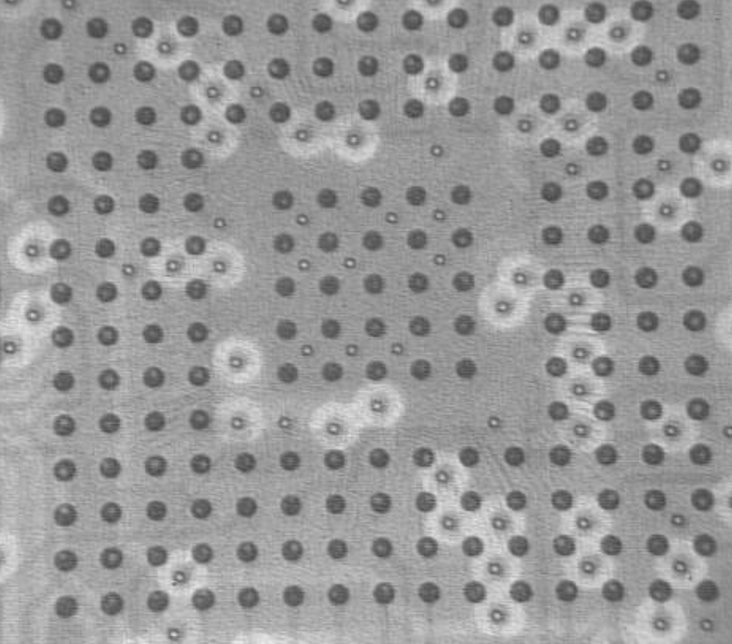
Identifying solder joint voids, especially within intricate components like BGAs, presents a significant challenge because these connections are hidden from direct view. Consequently, conventional visual inspection methods are largely ineffective, making advanced techniques like X-ray inspection an indispensable tool in the electronics manufacturing industry.
Principles of X-Ray Inspection
X-ray inspection systems employ high-resolution imaging technology to penetrate the layers of electronic components and PCBs, providing a detailed internal view of solder joints. Within these images, voids appear as darker areas because their lower density—being air pockets—absorbs fewer X-rays compared to the surrounding denser solder material. Contemporary X-ray equipment can identify voids as small as 5% of the total solder joint area, offering critical insights into their precise size, location, and distribution within the connection.
Advantages for BGA Void Analysis
For BGA components, X-ray inspection is uniquely valuable. It allows manufacturers to evaluate the quality of hundreds of solder joints concurrently without resorting to destructive testing methods. By meticulously analyzing void percentages and their patterns, engineers can establish correlations between observed defects and specific manufacturing process issues, such as problems with solder paste application or errors in the reflow profile. Adherence to industry benchmarks, such as those specified in IPC-A-610, which typically mandates void levels below 25% for BGA joints, is effectively monitored and ensured through X-ray examination.
Limitations and Supporting Techniques
While X-ray inspection is a powerful diagnostic tool, it does have some practical limitations. The process can be time-consuming for very large production batches, and accurately interpreting the detailed X-ray images demands skilled and experienced operators. In certain specialized situations, complementary methods like acoustic microscopy or destructive cross-sectioning might be employed to further validate findings or gain additional insights. However, for non-destructive, high-throughput inspection, X-ray technology remains the industry's preferred solution.
Strategies to Prevent Solder Joint Voids
Preventing solder joint voids requires a strategic, holistic approach that addresses every aspect from initial material selection to the optimization of manufacturing processes. Effective strategies often involve precise control over the reflow process and the application of specialized equipment.
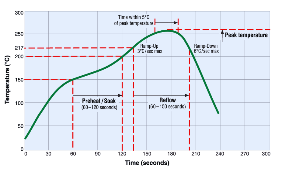
Optimizing Reflow Profiles
A meticulously designed reflow profile is one of the most effective tools for minimizing void formation. Such a profile ensures that the flux activates correctly, gases are adequately released, and the solder melts and flows optimally. Key aspects to consider for an effective reflow profile include:
● Preheat Phase: Gradually elevate the board's temperature to between 150-180°C over a period of 60-90 seconds. This phase is crucial for activating the flux and preventing sudden, aggressive outgassing.
● Soak Phase: Maintain the temperature between 150-200°C for 60-120 seconds. This allows sufficient time for volatile components in the solder paste to escape before the solder fully liquefies.
● Peak Phase: Achieve a peak temperature of 235-245°C (adjusted for the specific solder alloy) for 20-40 seconds. This ensures complete melting and proper wetting without exposing components to excessive heat.
● Cooling Phase: Control the cooling rate at 2-4°C per second. This prevents thermal shock and allows the solder joints to solidify with optimal microstructure.
Routinely testing different profiles and monitoring void levels using X-ray inspection can help in fine-tuning the process for specific BGA components or unique board designs.
Utilizing Vacuum Reflow Soldering
Vacuum reflow soldering represents an advanced technique specifically designed to significantly reduce solder joint voids. This method involves conducting the entire reflow process within a vacuum chamber, where the reduced atmospheric pressure facilitates the easier escape of trapped gases from the solder paste during outgassing. Studies have demonstrated that employing vacuum reflow can drastically lower void percentages in BGA joints, sometimes reducing them from 30% to less than 10%, which translates to substantial improvements in both mechanical robustness and thermal performance. While this technology demands specialized equipment and may entail higher production expenses, it is an invaluable approach for applications requiring the highest levels of reliability.
Controlling Solder Paste Application
Precise control over solder paste application is fundamental to minimizing voids. It is essential to utilize a stencil that is accurately designed to match the pad geometry, ensuring a consistent and uniform deposition of paste. Avoiding excessive paste application is crucial, as surplus material can trap more gases during the reflow process. Furthermore, selecting solder pastes formulated with low-voiding fluxes, specifically engineered to reduce outgassing, is highly recommended. Proper storage of solder paste at recommended temperatures (typically 2-10°C) and allowing it to acclimatize to room temperature before use also helps prevent moisture absorption, which can lead to subsequent voiding.
Enhancing PCB Design and Preparation
Thoughtful design choices play a significant role in preventing voids. For BGA components, integrating via-in-pad designs with effective plugging or capping is important to prevent air from becoming trapped. Optimizing pad sizes helps to achieve a balanced solder volume and promote adequate wetting. Prior to PCB assembly, it is beneficial to bake PCBs and components at temperatures between 100-125°C for 4-8 hours to eliminate any absorbed moisture, especially for moisture-sensitive devices. Thorough cleaning of all surfaces is also critical to remove contaminants that could impede proper solder flow.
Managing Flux Activity
While flux is indispensable for removing oxides and fostering good solder wetting, its activity level must be carefully balanced. Highly active fluxes can produce a greater volume of gases, thereby increasing the risk of void formation. It is advisable to collaborate with your solder paste supplier to select a formulation that offers moderate activity and leaves minimal residue, specifically tailored for BGA applications. Ensuring an even application of flux and avoiding any excess can further contribute to reducing voiding.
Practical Advice for Reducing Solder Joint Voids
Beyond the comprehensive strategies, several practical tips can further help in keeping solder voiding to a minimum during the PCB assembly process.
● Regularly calibrate reflow ovens to guarantee uniform temperature distribution and consistent profiles across all boards.
● Consider using a nitrogen atmosphere during the reflow process, which helps to reduce oxidation and enhance solder wetting characteristics.
● Implement periodic X-ray inspections on sample boards from production runs to identify early voiding trends and allow for timely process adjustments.
● Provide thorough training to operators on the correct handling and storage protocols for all materials to prevent contamination.
● Engage with material suppliers to rigorously test and validate low-voiding solder pastes specifically for your particular applications and production needs.
The Critical Impact of Voids on Electronic Reliability
Solder joint voiding is far more than a superficial defect; it directly impacts the functional performance and expected lifespan of electronic assemblies. Within BGA components, voids can severely impair heat dissipation, potentially leading to overheating in high-power applications. These structural weaknesses can also become points of concentrated stress, significantly increasing the risk of cracking when components are subjected to thermal cycling or mechanical shock. In highly critical sectors, such as medical devices or aerospace, where even minimal failure rates are unacceptable, stringent control over solder joint voids is absolutely essential. By diligently implementing the prevention and detection strategies discussed, void levels can be maintained well below the typical industry threshold of 25%, thus ensuring the creation of exceptionally robust and reliable connections.
Achieving Robust Solder Joints with AIVON
Solder joint voids, particularly prevalent in BGA assemblies, represent a notable challenge within the realm of electronics manufacturing. While their origins are diverse—ranging from solder paste outgassing to suboptimal reflow profiling—effective solutions are readily available. By embracing advanced inspection methods such as X-ray for identifying solder voids, and adopting preventive measures like vacuum reflow soldering and finely tuned reflow profiles, manufacturers can achieve superior quality and highly dependable solder joints.
At AIVON, we are dedicated to supporting your success through state-of-the-art assembly services and expert guidance. Whether your needs involve optimizing existing processes or require high-precision PCB manufacturing, our team is equipped to assist you in minimizing solder joint voids and enhancing overall product reliability. Partner with AIVON to build electronics designed for enduring performance.


