Introduction
Flexible printed circuit boards (FPCBs) have revolutionized electronic design by enabling compact, lightweight, and dynamically adaptable solutions. The inherent flexibility of these substrates, while offering numerous advantages, also introduces unique considerations and challenges during the assembly process. Unlike rigid PCBs, the assembly of flexible circuits demands specialized techniques, meticulous process control, and a deep understanding of material properties to ensure robust performance and reliability. This guide provides a comprehensive overview of the essential techniques and best practices for successful flexible PCB assembly.
What is Flexible PCB Assembly and Why it Matters
Flexible PCB assembly refers to the process of populating flexible substrates with electronic components, creating a functional circuit. FPCBs are constructed from thin, pliable dielectric materials, typically polyimide, which allows the circuit to bend, twist, and conform to various shapes.
The significance of flexible PCB assembly lies in its ability to facilitate miniaturization, reduce overall system weight, and enable three-dimensional interconnections in ways rigid boards cannot. This capability is critical for applications requiring compact designs, such as wearables, medical devices, automotive electronics, and aerospace systems. Proper flexible PCB assembly ensures that the delicate substrate and components withstand manufacturing stresses and deliver reliable performance throughout the product's lifespan, even under dynamic flexing conditions.
Challenges in Flexible PCB Assembly
The pliable nature of flexible circuits presents several distinct challenges during assembly that differentiate it from rigid PCB processing. Addressing these challenges is paramount for achieving high yield and product quality.
- Material Handling: Flexible substrates are delicate and susceptible to damage, creasing, or stretching during handling. Specialized equipment and careful operator training are essential to prevent physical defects. Electrostatic discharge (ESD) protection is also critical, as flexible materials can be prone to static charge buildup.
- Thermal Management: Flexible substrates, particularly polyimide, often have lower thermal resistance compared to FR-4 used in rigid PCBs. This requires precise control of temperature profiles during soldering processes to prevent material degradation, delamination, or discoloration.
- Dimensional Stability: FPCBs can exhibit greater dimensional changes (expansion or contraction) than rigid boards when subjected to thermal cycles. This variability can affect registration accuracy during printing, component placement, and subsequent reflow.
- Soldering Process: Achieving strong, reliable solder joints on a flexible substrate without causing damage or introducing excessive stress is a primary concern. The thinness of the substrate can lead to rapid heat transfer, potentially causing component tombstoning or lifting.
- Component Placement Accuracy: Ensuring precise component placement on a non-rigid surface requires robust fixturing and finely tuned automated equipment. Any localized movement of the substrate during placement can lead to misalignment.
- Warpage and Wrinkling: During thermal cycles, differential expansion between copper traces and the dielectric material can induce warpage, wrinkling, or buckling in the flexible circuit. This can compromise solder joint integrity and overall planarity.
Key Flexible PCB Assembly Techniques
Overcoming the inherent challenges of flexible materials requires a specialized approach throughout the assembly line.
Substrate Preparation and Panelization
Effective preparation begins with proper tooling. Flexible circuits are often supplied in panels with a frame or mounted on rigid carriers to provide mechanical stability during automated processing. This panelization allows for efficient handling through standard SMT equipment. For circuits requiring localized stiffening, such as where connectors or heavier components are mounted, rigidizers or stiffeners are precisely applied using heat-activated adhesives before component placement. Adherence to design standards like IPC-2223C ensures appropriate panel layout and handling features.
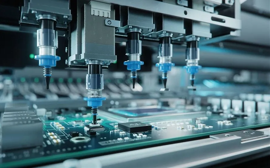
Component Placement Precision
Accurate component placement is a critical step in flexible PCB assembly. Due to the flexible nature of the substrate, specialized techniques are employed to maintain precision.
- Automated Component Placement: High speed pick and place machines are universally used for surface mount technology (SMT) assembly. These machines must be configured with gentle vacuum nozzles and controlled placement forces to avoid damaging the flexible material.
- Maintaining Flatness: Custom-designed support fixtures, pallets, or vacuum tables are essential to hold the flexible substrate perfectly flat and taut during the placement process. This rigidity ensures consistent placement accuracy.
- Fiducial Marks: Precisely etched fiducial marks on the flexible circuit are crucial for the optical alignment systems of pick and place machines. These marks compensate for minor dimensional changes or distortions in the flexible material.
Solder Paste Application
Applying solder paste onto flexible circuits requires careful consideration to ensure proper volume and alignment without deforming the substrate.
- Stencil Design: Stencils are typically laser-cut from stainless steel. For flexible PCBs, thinner stencils (e.g., 0.08 mm to 0.12 mm) may be used, and aperture designs might be adjusted to reduce the volume of paste for fine pitch components, helping to mitigate issues like bridging.
- Printing Process: Solder paste printing on flexible circuits demands precise squeegee pressure and speed settings. Excessive pressure can deform the flexible material, leading to inconsistent paste deposits. Vision systems are used to verify stencil-to-board alignment.
- Solder Paste Inspection (SPI): Three-dimensional SPI systems are vital for inspecting the volume, height, and shape of every solder paste deposit. This ensures quality before reflow and helps identify potential issues related to substrate flatness or stencil performance.
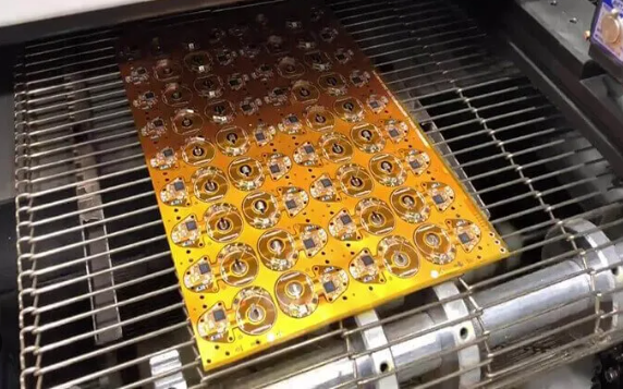
Reflow Soldering for Flexible PCBs
Reflow soldering is the primary method for attaching surface mount components to flexible circuits. This process is highly sensitive to the unique thermal properties of flexible substrates.
- Temperature Profiles: Developing an optimized reflow profile is crucial. Flexible substrates typically have lower thermal mass and can be more susceptible to thermal damage than rigid boards. Therefore, peak reflow temperatures are often reduced, and the preheat zone may be extended to allow for gradual heating. The cooling rate also needs careful management to prevent thermal shock.
- Support Fixtures: Custom reflow pallets or carriers are indispensable. These fixtures cradle the flexible circuit throughout the reflow oven, maintaining its flatness, preventing warpage, and minimizing shrinkage. They also help to evenly distribute heat across the flexible material.
- Nitrogen Atmosphere: Using a nitrogen inert atmosphere in the reflow oven can significantly improve solder joint quality by reducing oxidation. This is particularly beneficial for fine pitch components and dense assemblies on flexible circuits.
- Solder Alloys: Low temperature solder pastes, such as those incorporating bismuth-tin alloys, may be employed to reduce the overall thermal stress on the flexible substrate and components. This approach reduces the risk of material degradation and warpage. Industry standards like J-STD-001H provide guidelines for solder material selection and process controls.
Wave Soldering Considerations
Wave soldering is generally not recommended for most flexible PCB assemblies, especially those with surface mount components on both sides or delicate flex materials.
- Thermal Stress: Direct contact with molten solder subjects the flexible substrate to extreme thermal shock, which can cause severe warpage, delamination, or blistering.
- Molten Solder Contact: The continuous wave of molten solder can physically damage the thin, flexible material.
- Applicability: In rare cases, wave soldering may be considered for robust flex-rigid designs or for through-hole components on single-sided flexible circuits where the flexible material is specifically designed to withstand the thermal and mechanical stresses. However, even then, extensive process development and strict controls are necessary to prevent defects.
Manual Assembly and Rework
Despite high levels of automation, some components or specialized operations may require manual intervention. Rework on flexible circuits is particularly challenging.
- Specialized Tools: Low power soldering irons with fine tips and controlled temperature settings are essential. Thermal tweezers and hot air rework stations designed for delicate materials are also used.
- Substrate Protection: When performing manual soldering or rework, thermal barriers, Kapton tape, or localized heat sinks are applied to protect the surrounding flexible material from excessive heat.
- Adhesives: For attaching specific components, connectors, or additional stiffeners, specialized flexible adhesives might be used instead of or in conjunction with soldering.
Conformal Coating and Encapsulation
Once assembled, many flexible PCB assemblies benefit from protection against environmental factors.
- Environmental Protection: Conformal coatings, applied as thin polymeric films, protect the circuit from moisture, dust, chemicals, and extreme temperatures. Encapsulants provide even more robust physical protection.
- Flexibility Retention: The chosen coating or encapsulant must retain its flexibility after curing to ensure it does not crack or delaminate during the bending or flexing of the circuit. Acrylic, silicone, or polyurethane based coatings are often selected for their flexibility.
- Application Methods: Coatings can be applied via spraying, dipping, or selective coating processes, ensuring uniform coverage without compromising the flex characteristics.
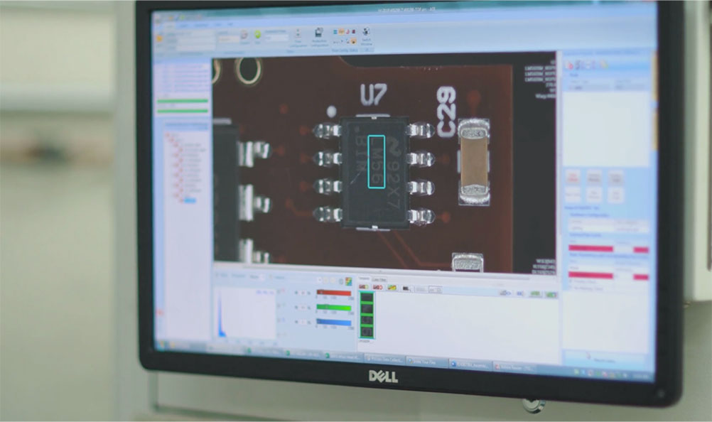
Quality Control and Inspection for Flexible PCB Assemblies
Rigorous quality control and inspection are paramount throughout the flexible PCB assembly process to ensure reliability and performance.
- Visual Inspection: Trained operators perform magnified visual inspections to check for solder defects, component misalignment, and any physical damage to the flexible substrate. Standards like IPC-A-610J provide criteria for acceptability of electronic assemblies.
- Automated Optical Inspection (AOI): AOI systems are crucial for rapidly and accurately inspecting component presence, polarity, placement, and solder joint quality on fine pitch components and complex assemblies. AOI can detect missing components, incorrect parts, and various solder defects.
- Electrical Testing: Functional tests, in-circuit tests (ICT), continuity checks, and isolation resistance tests verify the electrical performance of the assembled circuit.
- Flex Testing: For dynamic applications, specialized flex testing involves repeatedly bending or twisting the flexible circuit to simulate its operational environment. This helps validate the long term reliability of solder joints and the flexible material itself.
- X-ray Inspection: For components with hidden solder joints, such as BGAs (Ball Grid Arrays) and QFNs (Quad Flat No-leads), X-ray inspection is used to verify solder joint integrity and detect voids or shorts.
Conclusion
Flexible PCB assembly is a sophisticated process that demands a comprehensive understanding of material science, precise process control, and specialized equipment. By carefully managing material handling, optimizing thermal profiles during reflow soldering, ensuring accurate component placement, and implementing stringent quality control measures, manufacturers can overcome the inherent challenges of flexible substrates. The adoption of these specialized techniques ensures the production of high quality, reliable flexible electronic assemblies that meet the demanding requirements of modern electronic devices, thereby maximizing the benefits of flexible circuit technology.
FAQs
Q1: How does flexible PCB assembly differ from rigid PCB assembly?
A1: Flexible PCB assembly differs from rigid PCB assembly primarily in material handling and thermal management. Flexible substrates are more delicate and susceptible to damage, requiring specialized fixtures and gentle handling. Their lower thermal resistance necessitates precise reflow profiles to prevent material degradation.
Q2: What are the main challenges in reflow soldering flexible PCBs?
A2: The main challenges in reflow soldering flexible PCBs include preventing warpage and shrinkage, managing the lower thermal resistance of the substrate, and achieving consistent solder joint quality. Custom carriers, optimized temperature profiles, and sometimes low temperature solder pastes are used to mitigate these issues.
Q3: Can wave soldering be used for flexible PCB assembly?
A3: Wave soldering is generally not recommended for flexible PCB assembly due to the high thermal stress it imposes on the delicate substrate. The direct contact with molten solder can cause delamination, warpage, or material damage. It is typically only considered for very specific, robust flex-rigid designs or certain through-hole components.
Q4: What industry standards apply to flexible PCB assembly?
A4: Key industry standards applicable to flexible PCB assembly include IPC-2221A (Generic Standard on Printed Board Design), IPC-2223C (Sectional Design Standard for Flexible Printed Boards), IPC-A-610J (Acceptability of Electronic Assemblies), and J-STD-001H (Requirements for Soldered Electrical and Electronic Assemblies).
References
IPC-2221A — Generic Standard on Printed Board Design. IPC, 2003.
IPC-2223C — Sectional Design Standard for Flexible Printed Boards. IPC, 2017.
IPC-A-610J — Acceptability of Electronic Assemblies. IPC, 2024.
J-STD-001H — Requirements for Soldered Electrical and Electronic Assemblies. IPC & JEDEC, 2020.


