Introduction
Hand soldering and PCB layout are fundamental skills for electronic hobbyists looking to bring their projects to life. Whether assembling a simple circuit or prototyping a complex design, mastering these techniques ensures reliable connections and functional boards. For hobbyists working at home, challenges like limited tools and workspace can make the process daunting. This article explores practical methods for hand soldering, effective PCB layout strategies, and tips for home hand solder stencil placement. It also covers easy prototyping with stencil techniques to streamline your workflow. With a focus on actionable advice, this guide aims to help hobbyists achieve professional results using accessible tools and methods while adhering to industry best practices.
What Is Hand Soldering and PCB Layout?
Hand soldering involves manually joining electronic components to a printed circuit board using a soldering iron and solder material. It is a critical skill for hobbyists who often work on small scale projects or prototypes where automated assembly is not feasible. PCB layout, on the other hand, refers to the design and arrangement of components and traces on a board before manufacturing. A well planned layout minimizes errors during soldering and ensures the circuit functions as intended. For hobbyists, both processes are interconnected since a poor layout can complicate soldering, leading to issues like short circuits or weak joints. Understanding these skills is essential for creating reliable electronics at home.
Technical Principles of Hand Soldering
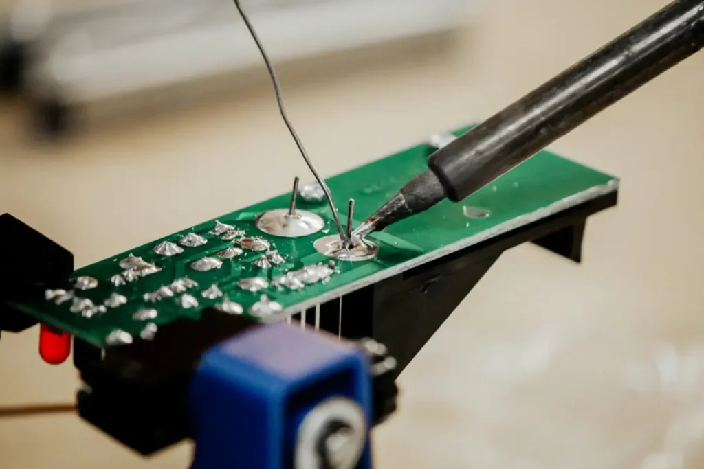
Hand soldering relies on the controlled application of heat to melt solder, forming a bond between components and PCB pads. The process requires a soldering iron with a suitable tip, typically between 25 to 40 watts for hobbyist use, to avoid overheating delicate parts. Solder, often a tin lead or lead free alloy, must wet the surfaces properly to create a strong joint. Flux, a chemical agent, is used to clean surfaces and promote solder flow, reducing oxidation during heating.
Temperature control is vital. Most components and boards can withstand temperatures around 300 degrees Celsius for a short duration, as outlined in industry standards like IPC J STD 020E for moisture and reflow sensitivity. Exceeding this can damage components or lift pads. Hobbyists should also be aware of cold solder joints, which occur when insufficient heat prevents proper bonding, resulting in unreliable connections. Using the right technique, such as heating the pad and component lead simultaneously before applying solder, ensures a solid joint.
For PCB layout, the technical focus is on spacing and trace routing. Adequate clearance between traces prevents short circuits, while proper pad sizes accommodate hand soldering without excess solder buildup. Standards like IPC 6012E for rigid printed boards provide guidelines on acceptable design tolerances that hobbyists can adapt for simpler projects. Keeping high current traces short and wide reduces resistance and heat buildup, which is crucial for safe operation.
Technical Principles of PCB Layout for Hand Soldering
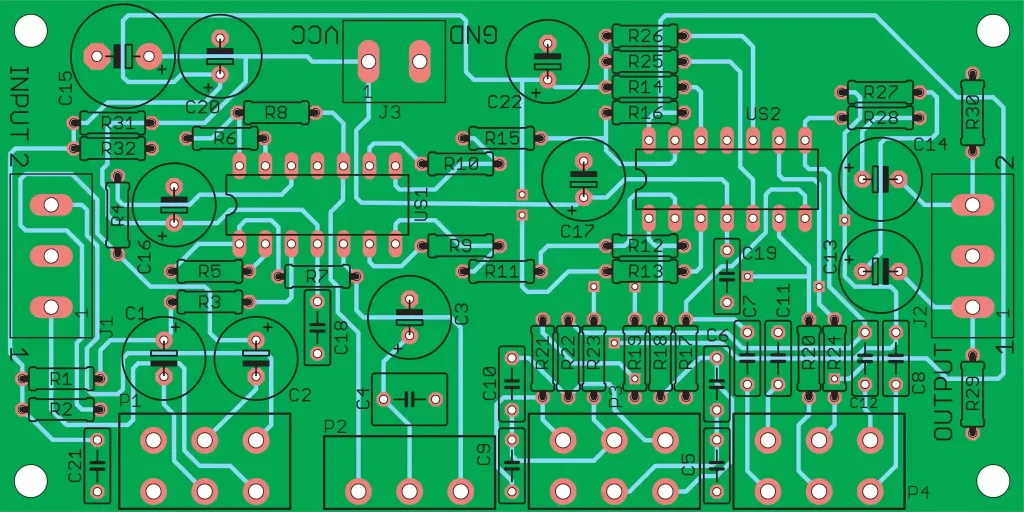
When designing a PCB layout for hand soldering, hobbyists must prioritize accessibility and simplicity. Components should be placed with enough spacing to allow a soldering iron tip to reach pads without touching adjacent parts. Small surface mount components, like 0805 resistors, require pads with clear boundaries to avoid solder bridging. Through hole components need larger pads and holes to accommodate manual insertion and soldering.
Routing traces also plays a role. Avoid sharp angles in traces as they can create weak points or complicate soldering. Keep signal traces away from power lines to reduce interference. For multilayer boards, ensure vias are placed where they can be accessed if rework is needed. Following design guidelines from standards like IPC A 600K for acceptability of printed boards helps hobbyists create layouts that are easier to assemble by hand.
Practical Solutions for Home Hand Solder Stencil Placement
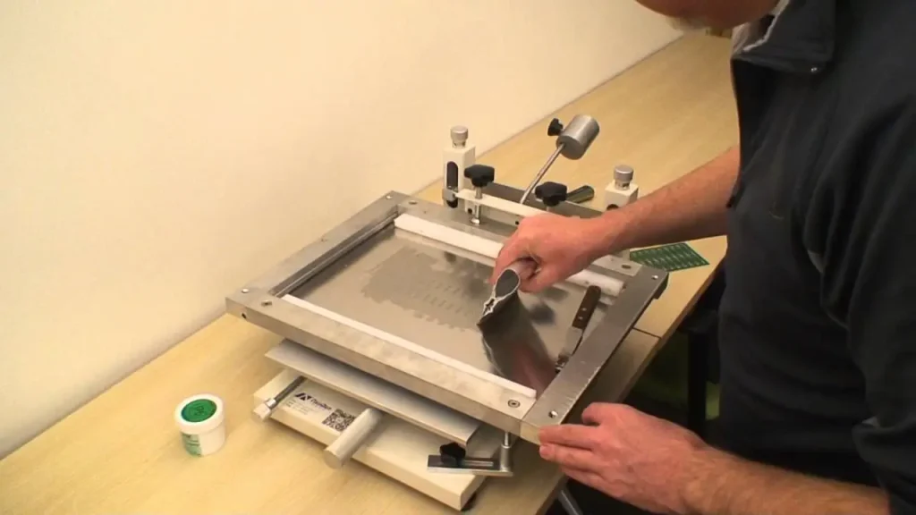
Stencil placement at home can simplify soldering surface mount components by ensuring precise solder paste application. Home hand solder stencil placement starts with selecting a stencil material, such as thin stainless steel or durable plastic, compatible with small scale projects. The stencil should match the PCB layout exactly, with openings aligned to the pads where solder paste will be applied.
To place the stencil, secure the PCB on a flat surface using tape or a simple jig. Align the stencil over the board by matching fiducial marks or board edges. If no fiducials exist, visually align using component outlines. Apply a small amount of solder paste using a squeegee or plastic card, spreading it evenly across the stencil openings. Lift the stencil carefully to avoid smudging the paste. This method works well for hobbyists without access to professional equipment.
For better accuracy, create a makeshift frame or use alignment holes on the stencil and board. As shared in posts found on social platforms, adding small holes or cutouts slightly larger than the board outline can aid in positioning. This approach to home hand solder stencil placement reduces errors and speeds up the process, especially for repetitive tasks.
After paste application, place components onto the paste using tweezers. Heat the board with a hot air gun or reflow oven if available, or use a soldering iron for manual touch up. Clean the stencil after each use to prevent paste buildup, ensuring consistent results for future projects.
Easy Prototyping with Stencil Techniques
Easy prototyping with stencil use transforms how hobbyists approach small batch PCB assembly. Stencils reduce the time spent on manually applying solder paste, especially for surface mount designs with multiple components. For prototyping, start with a single sided or double sided board design that matches your skill level and available tools.
Begin by ordering or creating a stencil with the same Gerber files used for the PCB. Many hobbyists use online services to obtain affordable stencils, ensuring the aperture sizes match pad dimensions as per design files. At home, secure the PCB and stencil as described earlier. Apply a thin layer of solder paste, focusing on even distribution to avoid excess or insufficient paste on pads.
Once components are placed, reflow soldering can be done using a low cost hot plate or toaster oven, monitoring the process to prevent overheating. If reflow equipment is unavailable, hand soldering with an iron can still work for small prototypes. Easy prototyping with stencil methods allows hobbyists to test designs quickly, iterate on layouts, and refine circuits without extensive rework.
For complex prototypes, consider breaking the design into smaller modules. Assemble and test each module separately using stencil applied paste before integrating them. This approach minimizes errors and makes debugging easier. Always inspect joints after soldering, looking for bridges or incomplete connections, and use a magnifying glass for fine pitch components.
Best Practices for Hand Soldering and Layout Design
To achieve reliable results, hobbyists should follow best practices tailored to their home setup. For hand soldering, always use a clean soldering iron tip. Tin the tip before each session by applying a thin layer of fresh solder to maintain heat transfer. Work in a well ventilated area to avoid inhaling fumes, and use a small fan if needed.
When soldering, apply heat to the pad and component lead together for two to three seconds before introducing solder. This ensures both surfaces are hot enough for the solder to flow evenly. Avoid excessive solder, as it can create blobs or bridges, especially on small pads. Use desoldering wick or a suction tool to remove excess solder if mistakes occur.
For PCB layout, prioritize component orientation. Place similar components in the same direction to simplify assembly and reduce errors. Group related components together, such as resistors near their corresponding ICs, to keep traces short. Leave ample space around connectors and switches for easy access during testing or use.
Test points are another useful feature in layouts. Add small pads at key circuit nodes to allow voltage or signal checks without disrupting soldered components. Label these points clearly on the silkscreen layer for quick identification. Following guidelines from standards like IPC 6012E ensures the design supports manual assembly without compromising performance.
Troubleshooting Common Hand Soldering Issues
Hobbyists often face challenges like cold joints, solder bridges, or lifted pads during hand soldering. A cold joint appears dull and uneven due to insufficient heat. To fix this, reheat the joint with a clean iron tip and apply fresh solder if needed. Ensure the iron is at the correct temperature for the solder type used.
Solder bridges occur when excess solder connects adjacent pads, creating a short circuit. Use desoldering wick to absorb the extra solder, and clean the area with isopropyl alcohol afterward. Prevent bridges by applying solder sparingly and using flux to control flow. Lifted pads, caused by overheating or mechanical stress, can be tricky. If a pad lifts, route a small wire to reconnect the component to the trace, securing it with adhesive if necessary.
For stencil related issues during prototyping, uneven paste application can lead to poor joints. Ensure the stencil is flat against the PCB and apply consistent pressure with the squeegee. If paste smears, clean the stencil and board before retrying. These troubleshooting steps help maintain quality in home projects.
Conclusion
Hand soldering and PCB layout are indispensable skills for electronic hobbyists aiming to create functional and reliable circuits. By understanding the technical principles of soldering, designing layouts with hand assembly in mind, and using techniques like home hand solder stencil placement, hobbyists can achieve professional results. Easy prototyping with stencil methods further simplifies the process, enabling faster iteration and testing. Adopting best practices and troubleshooting common issues ensures consistent success in small scale projects. With patience and the right approach, hobbyists can master these skills and bring their electronic ideas to fruition.
FAQs
Q1: How can I improve home hand solder stencil placement for small PCBs?
A1: For better home hand solder stencil placement, secure your PCB on a flat surface using tape or a custom jig. Align the stencil using board edges or fiducial marks, and apply solder paste evenly with a squeegee. Adding alignment holes to the stencil can enhance precision. Clean the stencil after each use to avoid paste buildup, ensuring consistent results for small projects.
Q2: What tools are essential for easy prototyping with stencil at home?
A2: Easy prototyping with stencil requires a basic setup including a stencil matching your PCB design, solder paste, and a squeegee or plastic card for application. Tweezers help place components, while a hot air gun or low cost hot plate aids reflow. A magnifying glass is useful for inspecting small joints, ensuring accuracy during home prototyping.
Q3: How do I avoid solder bridges during hand soldering at home?
A3: To prevent solder bridges while hand soldering, apply solder sparingly to pads and use flux to control flow. Heat the pad and component lead together briefly before adding solder. If a bridge forms, use desoldering wick to remove excess solder. Working with a clean iron tip also reduces the risk of unintended connections.
Q4: Why is PCB layout important for hand soldering success?
A4: PCB layout directly impacts hand soldering by determining component spacing and trace accessibility. A well designed layout with adequate pad sizes and clearances prevents short circuits and simplifies iron access. Grouping related components and avoiding sharp trace angles reduces errors, making manual assembly smoother for hobbyists working on custom projects.
References
IPC-6012E — Qualification and Performance Specification for Rigid Printed Boards. IPC, 2020.
IPC-A-600K — Acceptability of Printed Boards. IPC, 2020.
IPC J-STD-020E — Moisture/Reflow Sensitivity Classification for Nonhermetic Surface Mount Devices. IPC, 2014.


