Introduction
High-density interconnect (HDI) printed circuit boards enable compact electronics with superior performance in applications demanding miniaturization and high-speed signaling. The HDI PCB layer stackup forms the foundation of these designs, dictating signal integrity, thermal management, and manufacturing feasibility. Engineers must optimize layer count and routing to accommodate fine-pitch components like BGAs while controlling costs and reliability risks. This article explores HDI PCB stackup strategies, focusing on configurations such as the 2+N+2 HDI stackup and microvia stackup approaches. By understanding these elements, designers can achieve efficient signal routing and impedance control essential for modern devices. Proper stackup design directly impacts overall board performance and yield.
What Is HDI PCB Stack-Up and Why It Matters
An HDI PCB layer stackup refers to the precise arrangement of conductive layers, dielectrics, and vias in a multilayer board to support high wiring density. Unlike conventional PCBs, HDI stackups incorporate microvias, blind vias, and buried vias to connect layers without penetrating the entire board thickness. This structure allows for finer lines, smaller pads, and denser routing, critical for devices like smartphones, wearables, and automotive electronics. The relevance stems from escalating demands for faster data rates and smaller form factors, where traditional through-hole vias limit density. Optimizing the HDI PCB layer stackup ensures balanced electrical, mechanical, and thermal properties, preventing issues like crosstalk or delamination. For electric engineers, mastering stackup design translates to reliable prototypes and production boards.
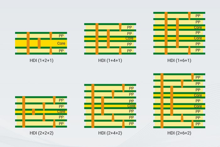
Key classifications include passive substrates with build-up layers on one or both sides, as outlined in industry guidelines. The 2+N+2 HDI stackup, for instance, features two microvia layers on each outer side flanking N inner core layers, ideal for moderate to high pin-count components. Microvia stackups further enhance this by staggering or stacking vias to maximize routing channels. Without thoughtful stackup planning, boards suffer from signal distortion or fabrication defects, underscoring its pivotal role in design success.
Technical Principles of HDI Stack-Up Design
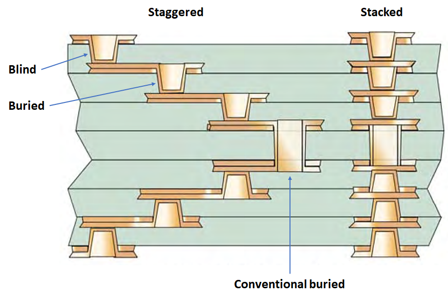
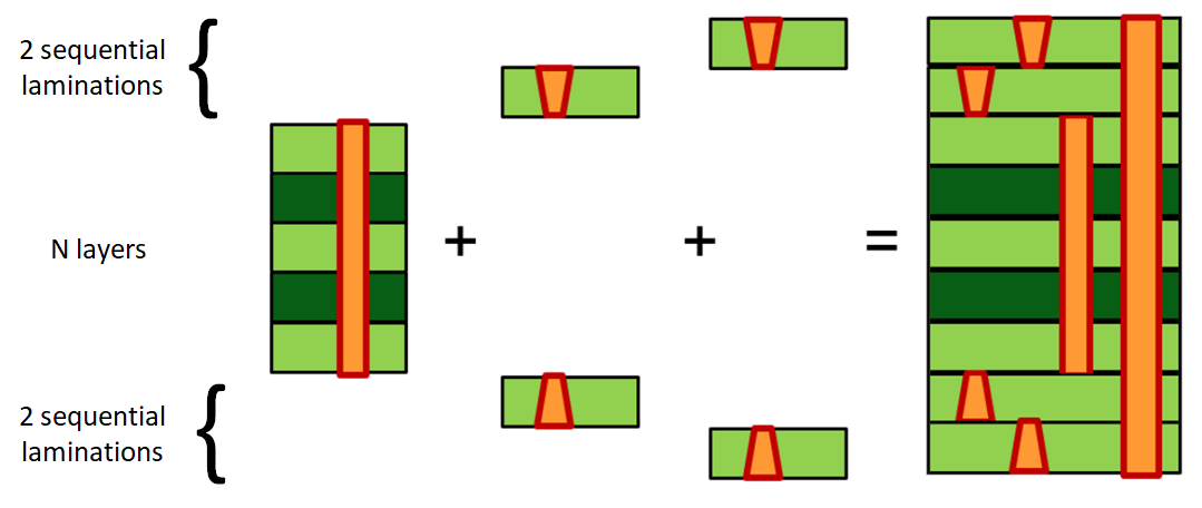
HDI stackups rely on sequential build-up processes, starting with a core laminate and adding thin dielectric layers with laser-drilled microvias. Microvias, typically under 150 microns in diameter, enable direct connections between adjacent layers, freeing up surface area for components. Stacked microvias connect multiple layers vertically, while staggered ones offset to avoid alignment stresses, influencing overall reliability. Layer count optimization balances routing density against thickness; excessive layers increase warpage risk due to CTE mismatches between copper and dielectrics. Signal routing benefits from this by allowing dog-bone escapes from fine-pitch BGAs directly into inner layers.
Impedance control in HDI PCB impedance control stackup demands symmetric construction with ground planes adjacent to signal layers. Dielectric thickness, trace width, and material permittivity dictate characteristic impedance, typically targeted at 50 ohms single-ended or 100 ohms differential. HDI stackup materials play a crucial role here, requiring low-loss resins with stable dielectric constants (Dk) and dissipation factors (Df) for high-frequency performance. Engineers calculate stackups using field solvers to predict impedance profiles across frequencies. Mechanical stability arises from matching CTE values across materials, minimizing via cracking during thermal cycling. These principles ensure the stackup supports both density and integrity.
IPC-2226 provides sectional design standards for HDI, emphasizing via formation, dielectric separation, and layer sequencing. Adhering to such guidelines prevents common pitfalls like via breakout failures.
Optimizing Layer Count in HDI Designs
Selecting the minimal viable layer count starts with component fanout requirements and routing escape analysis. A 1+N+1 stackup suits simpler BGAs with pitches above 0.65 mm, using one microvia layer per side. For denser arrays, the 2+N+2 HDI stackup becomes essential, adding a second microvia layer to handle sub-0.5 mm pitches by providing multiple escape rows. N represents the core layers, often 4 to 8 for signal routing and power distribution. This configuration optimizes by reducing board thickness compared to all-through-via alternatives, aiding in slim profiles. However, more build-up layers demand precise lamination control to avoid resin voids.
Trade-offs include cost escalation with each added microvia layer due to sequential processing, versus density gains in routing channels per mm^2. Engineers evaluate via-in-pad and filled vias to further condense space. Core thickness influences rigidity; thinner cores enable tighter bends but heighten warpage susceptibility. Simulation tools verify layer count adequacy by modeling routing completeness early in design. Ultimately, optimization yields boards with 20-50% higher density without proportional cost hikes.
Microvia Stackup and Signal Routing Strategies
Microvia stackup defines how vias interconnect layers, directly impacting routing efficiency. Staggered microvias alternate positions to distribute stresses, suitable for cost-sensitive designs with moderate reliability needs. Stacked microvias align vertically for maximum density, ideal for high-layer-count boards but requiring robust plating to withstand thermal stress. In a 2+N+2 HDI stackup, outer microvia pairs fan out signals to core planes, freeing the surface for components. Routing strategies leverage this by assigning high-speed nets to inner layers with stripline configurations for better shielding.
Blind and buried vias complement microvias by connecting non-adjacent layers without surface stubs, reducing inductance. Aspect ratios stay below 1:1 for microvias to ensure reliable plating. Signal routing prioritizes length matching and via staggering to minimize skew in differential pairs. Ground pour and plane splits manage return paths, crucial for impedance stability. These tactics enable escape routing under 0.4 mm BGA pitches, a hallmark of advanced HDI.
HDI PCB Impedance Control Stackup Considerations
Achieving consistent impedance in HDI demands a tailored HDI PCB impedance control stackup with uniform dielectric heights. Reference planes sandwich signal layers to form controlled impedance structures, suppressing radiation and crosstalk. Variations in prepreg thickness or copper weight disrupt this, necessitating test coupons for validation. Low-profile copper foils reduce skin effect losses at GHz frequencies. HDI stackup materials selection focuses on resins with Dk around 3-4 and low Df for minimal insertion loss.
Symmetry from top to bottom prevents camber, aiding flatness during reflow. Power integrity integrates with stackup by dedicating planes for decoupling. IPC-6016 outlines qualification tests for HDI performance, including impedance verification via TDR measurements. Engineers iterate stackups balancing these factors for target tolerances like +-10%.
Best Practices for HDI Stack-Up Implementation
Begin with a symmetric build-up to equalize copper distribution and minimize warpage. Select HDI stackup materials with matched CTE to copper, typically 15-20 ppm/C, for via reliability. Limit microvia depth to one or two layers per stack to avoid fill voids. Incorporate filled vias for planar surfaces under BGAs. Perform DFM reviews focusing on drill aspect ratios and panel utilization.
Layer sequencing places high-speed signals between planes, power/ground alternately. Use build-up dielectrics thinner than cores for microvia integrity. Validate with cross-sections per IPC standards. These practices enhance yield and performance.
Common Challenges and Troubleshooting Insights
Warpage arises from asymmetric CTE or lamination imbalances, detectable via shadow moire testing. Mitigate by core compensation or constrained build-ups. Signal integrity issues like ringing stem from via stubs; eliminate with blind vias. Thermal management challenges in high-layer counts require embedded planes and vias for heat spreading. Troubleshooting involves CAE simulations and early prototypes. Case insights from dense server boards show 2+N+2 stackups reducing layer count by 25% versus standard multilayers.
Conclusion
Optimizing HDI PCB layer stackup through strategic layer count, microvia configurations, and material choices unlocks superior density and performance. Configurations like the 2+N+2 HDI stackup exemplify efficient signal routing for demanding applications. Impedance control remains paramount, guided by precise stackup planning. Adhering to standards ensures manufacturability and reliability. Electric engineers benefit from these principles in delivering robust designs. Future trends point to even finer features, reinforcing stackup's centrality.
FAQs
Q1: What is a 2+N+2 HDI stackup?
A1: The 2+N+2 HDI stackup consists of two microvia build-up layers on each side of N core layers, enabling high-density routing for fine-pitch components. Microvias provide short, low-inductance paths, ideal for BGA escapes. This structure per IPC-2226 supports balanced signal integrity and mechanical stability. It optimizes layer count for moderate complexity boards.
Q2: How does microvia stackup affect HDI PCB layer stackup design?
A2: Microvia stackup determines via staggering or stacking, influencing routing density and stress distribution in HDI PCB layer stackup. Staggered setups reduce costs, while stacked enhance density. Proper implementation minimizes thermal fatigue. Designers select based on reliability needs.
Q3: Why is impedance control critical in HDI PCB impedance control stackup?
A3: Impedance control in HDI PCB impedance control stackup maintains signal quality by matching trace geometry to dielectrics and planes. It prevents reflections in high-speed nets. Symmetric layers ensure consistency. Test structures verify tolerances.
Q4: What HDI stackup materials are best for high-performance designs?
A4: HDI stackup materials prioritize low Dk/Df resins with CTE matching for microvia reliability. Thin build-up dielectrics support fine features. Selection impacts loss and speed. Standards guide qualification.
References
IPC-2226 - Sectional Design Standard for High Density Interconnect (HDI) Printed Boards. IPC, 2001 (revised 2017 as IPC-2226A)
IPC-6016 - Qualification and Performance Specification for High Density Interconnect (HDI) Layers and Boards. IPC, 2007 (current revisions apply)
IPC-6012E - Qualification and Performance Specification for Rigid Printed Boards. IPC, 2015


