Introduction
In modern high-speed electronics, signal integrity challenges dominate PCB design efforts. Engineers face issues like crosstalk, reflections, and electromagnetic interference as data rates climb into the gigahertz range. Buried vias emerge as a critical solution, acting as concealed pathways that connect inner layers without disrupting surface routing. These vias enable denser PCB inner layer routing while preserving signal quality. By minimizing parasitic effects, buried vias support faster signal propagation and reduced noise coupling. This article explores how buried vias optimize signal integrity, offering practical insights for electric engineers tackling complex multilayer boards.
What Are Buried Vias and Why Do They Matter for Signal Integrity?
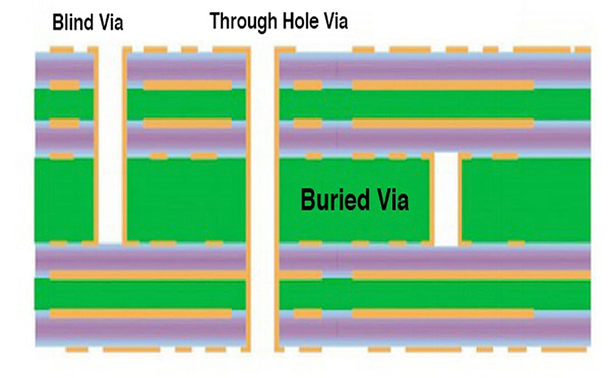
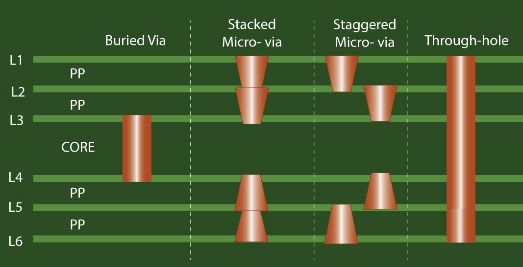
Buried vias are plated through-holes that connect two or more inner layers of a multilayer PCB, remaining entirely hidden from the outer surfaces. Unlike through-hole vias that span the full board thickness or blind vias that reach from one surface to an inner layer, buried vias avoid exposure to the top and bottom planes. This design choice becomes essential in high-density interconnects where surface space is premium. For signal integrity, buried vias reduce stub lengths, which are unused portions of vias that cause signal reflections. Shorter stubs mean less impedance discontinuity, allowing cleaner high-frequency signals to travel with minimal distortion.
The relevance intensifies in applications like telecommunications and computing, where buried vias crosstalk reduction proves vital. Crosstalk occurs when signals from adjacent vias or traces induce noise in neighboring paths. Buried vias, positioned deep within the stackup, experience less coupling to surface traces and components. This isolation enhances overall board performance, particularly in controlled impedance environments. Engineers prioritize them to meet rising demands for data throughput without expanding board size. Ultimately, buried vias signal integrity benefits translate to reliable operation in dense, fast circuits.
Technical Principles Behind Buried Vias and Signal Integrity
Signal integrity hinges on maintaining consistent impedance along transmission lines, and vias introduce potential mismatches. In through vias, the stub beyond the signal layer acts as a resonant element, reflecting energy back toward the source at frequencies where the stub length equals a quarter wavelength. Buried vias eliminate this stub for inner layer connections, ensuring the via length matches only the distance between connected layers. This precision reduces return loss and insertion loss, critical metrics in high-speed designs. Engineers model these effects using time-domain reflectometry or vector network analyzers to verify performance.
Crosstalk mechanisms further underscore buried vias advantages. Near-end crosstalk arises from mutual inductance between closely spaced vias, while far-end crosstalk stems from capacitive coupling. By routing signals on inner layers via buried vias, the physical separation from surface aggressors increases, damping these effects. Ground planes adjacent to signal layers shield further, confining fields within the board core. PCB inner layer routing with buried vias thus permits tighter spacing without proportional crosstalk rise. Quantitative analysis shows crosstalk voltage drops exponentially with separation, favoring inner placements.
Fabrication processes influence via reliability under thermal and mechanical stress. Sequential lamination builds stackups incrementally, allowing buried vias in specific core sections. This method ensures uniform plating thickness and void-free barrels, per IPC-6012E guidelines for rigid printed boards. Aspect ratios, defined as board thickness to via diameter, must stay below recommended limits to prevent plating defects. Engineers calculate these to balance density and manufacturability. Proper stackup symmetry also mitigates warpage, preserving via integrity during reflow cycles.
Thermal expansion mismatches between copper plating and dielectric materials generate stress at via interfaces. Buried vias, embedded in stable inner cores, endure less cycling exposure than surface vias. Reliability testing per IPC standards confirms their robustness in temperature-humidity biased environments. Signal propagation delay minimizes due to shorter paths, aiding timing budgets in synchronous designs. These principles collectively position buried vias as enablers of advanced signal integrity.
Best Practices for Buried Vias in PCB Inner Layer Routing
Effective implementation starts with stackup planning, allocating dedicated signal layers flanked by ground planes. This configuration provides return paths close to signals, stabilizing impedance at 50 or 100 ohms as needed. Buried vias should target minimal diameter feasible for the fabricator, typically 0.15 mm or larger, to ensure reliable drilling and plating. Spacing rules mandate at least three times the via diameter between adjacent vias to curb crosstalk. Engineers simulate routing density early, optimizing layer count for buried vias signal integrity.
During layout, prioritize PCB inner layer routing for high-speed nets, reserving surfaces for lower frequency or power distribution. Use teardrops at via-to-trace junctions to avoid etch undercuts and maintain current carrying capacity. Fanout patterns for buried vias benefit from staggered arrangements, reducing parallel run lengths that amplify coupling. Verification involves design rule checks for annular ring sizes and breakout reliefs. Post-layout, extract parasitics for signal integrity simulations, iterating if discontinuities exceed margins.
Manufacturing considerations demand clear documentation of via locations in fabrication drawings. Specify sequential build for boards exceeding eight layers, enabling precise buried via placement. Laser drilling suits microvias, but mechanical for standard buried vias offers cost efficiency. Aspect ratios under 10:1 align with IPC-2221 design standards, minimizing barrel cracks. Bake-out processes remove moisture before lamination, preventing voids. Final inspection via cross-sectioning validates fill and alignment.
Troubleshooting focuses on common pitfalls like impedance variation from asymmetric stackups. Warpage induces via strain, detectable through shadow moiré analysis. Adjust core thicknesses for balance, ensuring CTE matching across materials. If crosstalk persists, increase plane stitching density around vias. Field solvers quantify improvements, guiding refinements. These practices ensure buried vias crosstalk reduction translates to production success.
Real-World Insights: Troubleshooting Buried Vias in High-Density Designs
Consider a scenario where a 12-layer board exhibits eye closure at 10 Gbps despite simulations. Initial diagnosis points to via stub remnants from misaligned inner layers. Cross-sections reveal plating voids, traced to excessive aspect ratios violating fabricator capabilities. Corrective action involves downsizing vias and redistributing signals to shallower buried vias. Post-revision testing shows improved jitter margins, affirming buried vias signal integrity gains.
Another frequent issue arises in routing congestion, forcing buried vias near edges where support is thin. Mechanical stress during depaneling cracks barrels, leading to opens. Mitigation employs edge beveling and reinforced coupons for process control. Signal simulations incorporating tolerance stacks predict worst-case performance. Engineers document lessons in design libraries, standardizing templates for future projects. These insights highlight proactive verification's role.
Conclusion
Buried vias represent a cornerstone in optimizing signal integrity for multilayer PCBs. Their ability to facilitate PCB inner layer routing without surface intrusion slashes crosstalk and reflections. Engineers leveraging these vias achieve higher densities and speeds while adhering to proven principles. Best practices in design, simulation, and fabrication unlock their full potential. As board complexities grow, buried vias will remain indispensable for reliable high-performance electronics.
FAQs
Q1: What role do buried vias play in buried vias signal integrity?
A1: Buried vias enhance signal integrity by eliminating stubs that cause reflections in through vias. They maintain consistent impedance across inner layers, reducing insertion loss at high frequencies. Shielded by ground planes, they minimize EMI susceptibility. This setup supports clean eye diagrams in gigabit applications, essential for electric engineers designing fast interfaces.
Q2: How do buried vias contribute to crosstalk reduction?
A2: Buried vias crosstalk reduction stems from their inner positioning, increasing separation from surface aggressors. Mutual inductance drops with distance, confining fields between planes. Optimal spacing and staggering further suppress near- and far-end coupling. Simulations confirm voltage noise below 1% in dense routings, improving bit error rates.
Q3: What are key considerations for PCB inner layer routing with buried vias?
A3: PCB inner layer routing with buried vias requires symmetric stackups for warpage control and impedance stability. Limit via diameters to manufacturable sizes with aspect ratios under 10:1. Prioritize high-speed nets internally, using ground stitching for return paths. Verify with parasitic extraction to ensure timing and noise margins.
Q4: When should engineers choose buried vias over blind vias?
A4: Opt for buried vias when connecting multiple inner layers without surface access, ideal for dense signal planes. Blind vias suit surface-to-inner transitions but add complexity. Buried vias excel in crosstalk-sensitive designs due to full embedding. Balance with layer count and cost, per IPC guidelines.
References
IPC-6012E — Qualification and Performance Specification for Rigid Printed Boards. IPC, 2017
IPC-2221B — Generic Standard on Printed Board Design. IPC, 2012
IPC-A-600K — Acceptability of Printed Boards. IPC, 2020


