Introduction
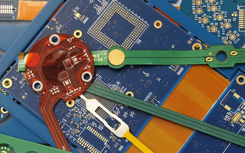
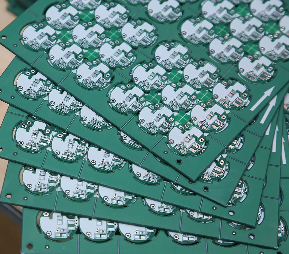
High-density interconnect (HDI) PCBs represent a critical advancement in PCB manufacturing, enabling the creation of compact medical devices that demand superior miniaturization and performance. These boards achieve higher wiring density per unit area compared to conventional PCBs, incorporating features like microvias and fine-line traces essential for space-constrained applications. In the medical field, where devices such as wearable monitors and portable diagnostics must integrate complex circuitry into tiny footprints, optimizing high interconnect density manufacturing becomes paramount. Factory-driven processes must balance throughput with reliability to meet growing demands for compact medical devices. This article explores the principles, challenges, and best practices for enhancing manufacturing density interconnect in HDI production tailored to medical needs. Engineers benefit from understanding these strategies to ensure scalable production without compromising quality.
What Are High-Density Interconnect PCBs and Why They Matter for Compact Medical Devices
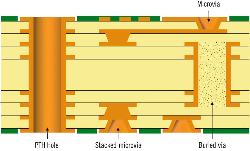
High-density interconnect PCBs, as defined by industry standards, feature microvias smaller than 150 microns, blind and buried vias, and finer line widths to pack more functionality into smaller areas. According to IPC-2226, HDI boards support structures like 1-n-1 or 2-n-1 stackups, where n represents core layers, allowing passive or active via configurations. These designs reduce signal path lengths, minimize electromagnetic interference, and support high-pin-count components critical for compact medical devices. In medical applications, such as implantable sensors or handheld ultrasound units, HDI enables integration of processors, sensors, and power management in volumes under a few cubic centimeters. Without HDI, traditional PCBs would require larger boards, increasing device size and patient discomfort. Optimizing PCB manufacturing for these boards ensures reliable performance in harsh biological environments.
The relevance of HDI intensifies with the push for miniaturized healthcare tech, where compact medical devices must withstand sterilization, vibration, and thermal cycling. Manufacturing density interconnect allows factories to produce boards with via-in-pad technology, supporting bottom-terminated components for even tighter layouts. This capability directly impacts device portability and battery life, key factors in patient compliance. Engineers designing for medical OEMs prioritize HDI to meet form factor constraints while maintaining signal integrity. Factory insights reveal that early adoption of HDI processes correlates with faster time-to-market for next-generation devices. Ultimately, high interconnect density manufacturing bridges design innovation with production scalability.
Key Technical Principles of HDI PCB Manufacturing
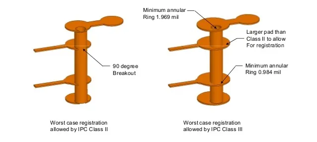
HDI PCB manufacturing relies on sequential lamination to build layers with precise microvia interconnections. Laser drilling creates blind and buried microvias in thin dielectric materials, typically resin-coated copper foils under 50 microns thick, ensuring aspect ratios below 1:1 for reliable plating. Filled vias, either electroplated copper or conductive epoxy, prevent voids that could compromise thermal or electrical performance in compact medical devices. Build-up processes alternate dielectric application, via formation, and patterning, demanding tight control over registration to align features across multiple layers. These principles enable higher routing density, but require specialized equipment for UV or CO2 laser ablation suited to material types. Factory alignment with standards like IPC-6012DS ensures qualification through thermal stress and reliability testing.
Material selection plays a pivotal role, favoring low-coefficient of thermal expansion (CTE) resins to match copper and prevent warpage during reflow. Thin cores and prepregs support finer pitches down to 40 microns, while surface finishes like ENIG provide flatness for fine-pitch BGAs common in medical electronics. Via staggering or stacking configurations distribute stress, enhancing mechanical integrity under flexing conditions found in wearables. Plasma cleaning precedes plating to remove drill smear, boosting adhesion and yield in high interconnect density manufacturing. Engineers must consider these mechanisms to avoid common pitfalls like via cratering from improper drilling parameters. Overall, these technical foundations allow manufacturing density interconnect at scale for demanding applications.

Challenges in High-Density Interconnect Manufacturing for Compact Medical Devices
Producing HDI PCBs for compact medical devices introduces challenges like maintaining yield amid complex via structures and multilayer builds. Sequential lamination increases cycle times, as each build-up cycle involves lamination, drilling, and plating, potentially bottlenecking throughput in high-volume runs. Microvia reliability under thermal excursions poses risks, with unfilled or poorly filled vias susceptible to cracking in medical sterilization processes. Registration accuracy across thin layers demands advanced imaging systems to prevent misalignment, which could short circuits in dense routing. Factories face panel utilization issues, where smaller board sizes for compact medical devices reduce economies of scale unless panel size optimization is applied. Balancing these factors requires process controls aligned with J-STD standards for soldering reliability.
Another hurdle is material handling for thin dielectrics, prone to handling damage or contamination, impacting surface quality for component mounting. High interconnect density manufacturing amplifies defect propagation, where a single via failure cascades through stacked structures. Yield data from production runs highlights the need for in-line monitoring, such as automated optical inspection after each lamination step. For medical devices, traceability from raw materials to finished boards ensures compliance with quality systems. Engineers must collaborate with fabricators early to mitigate design-induced challenges like excessive via density in fanout areas. Addressing these systematically optimizes capacity while upholding the stringent reliability needed for life-critical applications.
Best Practices for Optimizing Manufacturing Capacity in HDI PCBs
To optimize manufacturing capacity, factories implement design for manufacturability (DFM) reviews focusing on via fill completeness and stackup symmetry. Standardizing HDI classes, such as Class 3 for medical reliability, guides process parameters for consistent plating thickness over microvias. Panelization strategies maximize array density, incorporating breakaway tabs and fiducials for precise depaneling without stressing fine features. Automation in laser drilling and electroplating reduces variability, boosting throughput for compact medical devices production. Yield enhancement comes from statistical process control, monitoring aspect ratios and etch uniformity to preempt defects. These practices enable high interconnect density manufacturing at higher volumes.
Process sequencing prioritizes filled vias in inner layers to support outer layer patterning without collapse risks. Selecting dielectric materials with uniform drillability minimizes taper variations, ensuring clean via walls for plating. In-line metrology, including cross-section analysis on coupon strips, verifies via quality before full production. For manufacturing density interconnect, factories calibrate equipment for batch consistency, reducing setup times between runs. Collaboration on netlist verification catches routing errors pre-production, streamlining PCB manufacturing workflows. Implementing these best practices scales capacity reliably for compact medical devices.
Thermal management during lamination prevents resin flow inconsistencies, critical for void-free builds. Post-plating planarization ensures flatness for lithography, supporting sub-50 micron features. Factories leverage sequential build documentation to trace process deviations, facilitating continuous improvement. These factory-driven insights align production with medical-grade requirements, optimizing overall capacity.
Case Study Insights: Scaling HDI for Portable Medical Diagnostics
In a typical scenario for compact medical devices, a portable blood analyzer required an HDI PCB with 12-layer 2-10-2 stackup to integrate microfluidics controls and sensors. Initial prototypes faced yield issues from staggered microvia misalignment, addressed by enhancing fiducial density and laser registration. Optimizing panel size to 18x24 inches allowed 12-up arrays, doubling throughput while maintaining IPC-compliant tolerances. Via filling with copper electroplating improved thermal cycling endurance, vital for field use. Production scaled to 5,000 units monthly by automating inspection, demonstrating how targeted optimizations enhance manufacturing density interconnect. This approach underscores practical gains in high interconnect density manufacturing.
Conclusion
High-density interconnect PCBs are indispensable for compact medical devices, demanding optimized manufacturing capacity to deliver reliability and performance. Key principles like microvia technologies and sequential lamination form the backbone, while challenges in yield and throughput require proactive best practices. Factory strategies such as DFM, automation, and process controls ensure scalable PCB manufacturing. Engineers gain from standard-aligned approaches to achieve dense interconnects without trade-offs. As medical tech evolves, mastering these elements positions production for future demands. Prioritizing these insights drives efficient high interconnect density manufacturing.
FAQs
QX: What role does IPC-2226 play in high interconnect density manufacturing?
AX: IPC-2226 provides sectional design standards for HDI PCBs, specifying microvia rules, stackup types, and fine-feature tolerances. It ensures designs support reliable manufacturing density interconnect by defining limits on via sizes and layer builds. Factories use it to qualify processes for compact medical devices, reducing iteration cycles. Compliance enhances yield in complex structures.
QX: How can factories improve throughput for compact medical devices using HDI?
AX: Optimizing panel arrays and automating laser drilling sequences boosts throughput in PCB manufacturing. Sequential lamination efficiency improves with standardized build cycles and in-line yield monitoring. For high interconnect density manufacturing, via fill verification prevents downstream defects. These steps scale production reliably for medical volumes.
QX: Why are filled microvias essential in manufacturing density interconnect for medical PCBs?
AX: Filled microvias provide planar surfaces for subsequent layers, preventing voids that compromise reliability in compact medical devices. Electroplating or paste filling withstands thermal stress from sterilization. This practice aligns with standards for high interconnect density manufacturing, ensuring mechanical integrity. Factories prioritize it for multilayer HDI stability.
QX: What DFM considerations optimize HDI PCB manufacturing capacity?
AX: DFM emphasizes symmetric stackups, adequate fanout spacing, and material CTE matching to minimize warpage. Fiducial placement aids registration in high density interconnect processes. Early reviews catch issues, enhancing yield for compact medical devices. These ensure efficient PCB manufacturing scale-up.
References
IPC-2226A — Sectional Design Standard for High Density Interconnect (HDI) Printed Boards. IPC, 2017
IPC-6012DS — Qualification and Performance Specification for High Density Interconnect (HDI) Printed Boards. IPC, 2020
J-STD-001H — Requirements for Soldered Electrical and Electronic Assemblies. IPC, 2018