Introduction
High-Tg PCB assembly demands precise control during high-temperature soldering to ensure reliability in demanding applications. Electric engineers often face challenges with lead-free reflow processes that push temperatures beyond standard material limits, leading to potential warpage or delamination. High-Tg materials, with glass transition temperatures above 170°C, provide the thermal stability needed to withstand these conditions without compromising structural integrity. This article explores best practices for High-Tg PCB soldering temperature management, reflow profiles, solder paste selection, component placement, and the overall assembly process. By following these guidelines, engineers can minimize defects and achieve consistent yields. Practical insights grounded in industry standards help troubleshoot common issues effectively.
What Is High-Tg PCB Assembly and Why It Matters
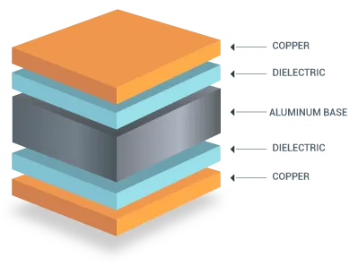
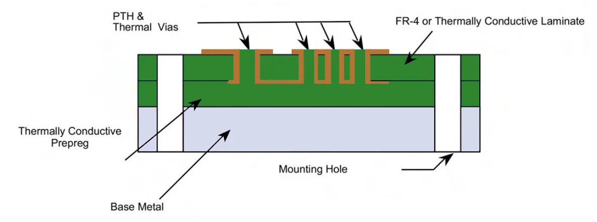
High-Tg PCB assembly involves surface-mount technology processes tailored for printed circuit boards using laminates with elevated glass transition temperatures. These materials maintain rigidity during exposure to elevated soldering temperatures, unlike standard FR-4 which softens around 130-140°C. In high-temperature soldering, the board must endure peak reflow temperatures without excessive deformation that could misalign components or cause open joints. This capability proves critical for automotive, aerospace, and power electronics where thermal cycling occurs post-assembly. Engineers specify high-Tg to align with component moisture sensitivity requirements and ensure long-term performance under heat stress. Neglecting these factors risks yield losses and field failures, making informed assembly practices essential.
Technical Principles Behind High-Temperature Soldering on High-Tg PCBs
During reflow soldering, the High-Tg PCB assembly process subjects the board to a thermal profile with preheat, soak, reflow, and cool-down phases. Above the glass transition temperature, the resin matrix transitions from glassy to rubbery state, reducing modulus and increasing warpage risk if copper distribution is unbalanced. High-Tg formulations delay this transition, preserving dimensional stability up to 260°C peaks common in lead-free alloys. Thermal expansion coefficient mismatches between copper layers and substrate exacerbate stresses, particularly in multilayer stacks. Moisture absorbed in the laminate vaporizes rapidly during ramp-up, potentially causing delamination if not preconditioned. Understanding these mechanisms allows engineers to optimize profiles and prevent tombstoning or bridging defects.
Component lead melting and paste flux activation occur within narrow windows, requiring precise ramp rates to avoid overheating sensitive parts. High-Tg boards exhibit lower hygroscopicity, aiding moisture control per IPC/JEDEC J-STD-020 guidelines for reflow sensitivity classification. Warpage measurements, typically below 0.75% for reliable assembly, depend on symmetric stack-up and fixture use during cooling. These principles guide troubleshooting, such as analyzing X-ray images for voiding patterns linked to rapid cooling.
Best Practices for High-Tg PCB Solder Paste Selection
Selecting the right High-Tg PCB solder paste starts with alloys compatible with peak reflow temperatures, such as tin-silver-copper variants designed for thermal stability. Engineers should choose pastes with fine particle sizes for high-density boards to improve printability and reduce voids. Flux activity must balance residue minimization with activation at preheat temperatures around 150-180°C. Storage at controlled refrigeration followed by room-temperature equilibration prevents slumping during stencil printing. Viscosity testing ensures consistent deposit volume across pad geometries. Troubleshooting paste issues involves inspecting stencil apertures for release efficiency and adjusting squeegee pressure.
In practice, no-clean fluxes suit high-Tg assemblies by leaving benign residues that withstand subsequent cleaning steps. Paste life post-printing demands monitoring to avoid oxidation, which degrades wetting. Integrating these choices into the High-Tg PCB assembly process enhances joint integrity and reduces rework.
Optimizing High-Tg PCB Reflow Profile
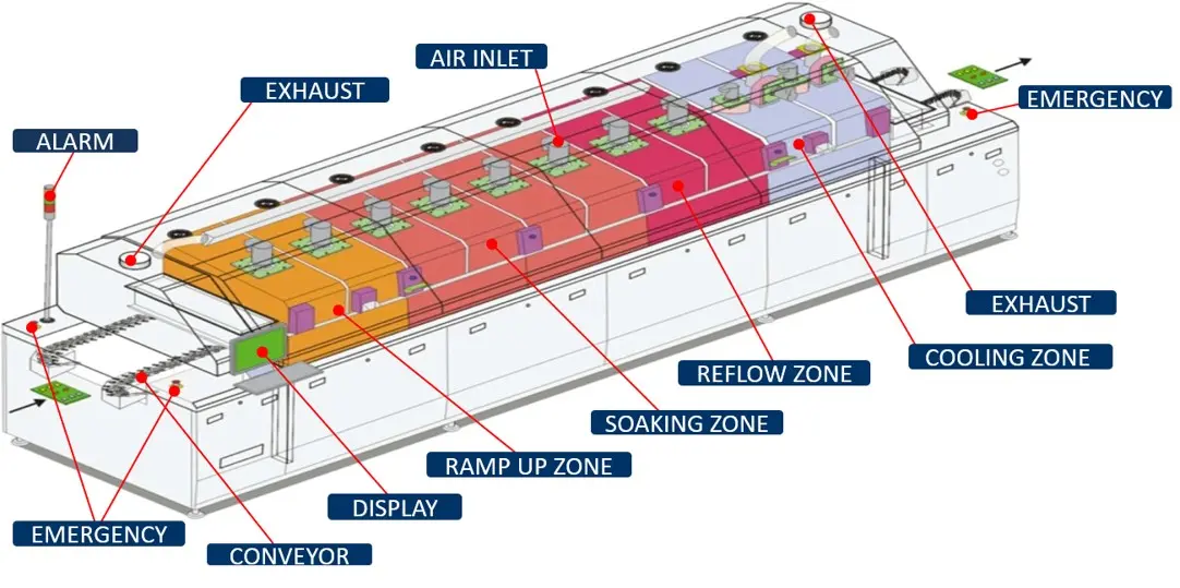
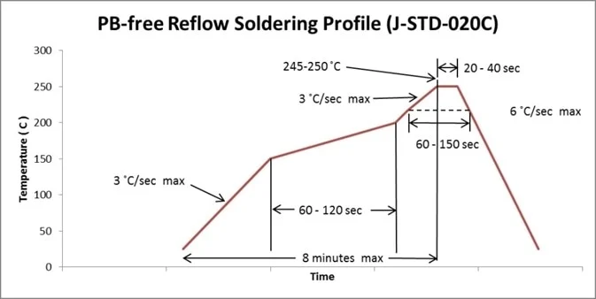
The High-Tg PCB reflow profile must adhere to established thermal ramps to protect both board and components from thermal shock. Preheat phases gradually raise temperatures to evaporate solvents without rapid flux burnout, typically ramping 1-3°C per second. Soak periods allow uniform heating, minimizing delta-T across thick boards. Peak High-Tg PCB soldering temperature exposure above liquidus (217°C for SAC alloys) lasts 40-90 seconds, with time above 220°C controlled per component classifications. Cooling rates below 6°C per second prevent brittle intermetallics. Profile validation uses thermocouples placed at critical locations like corners and centers.
Adjustments for high-Tg materials include extended soaks to equalize temperatures in denser copper planes. Nitrogen atmospheres reduce oxidation at peaks, improving wetting on high-Tg surfaces. Per IPC/JEDEC J-STD-020, profiles classify moisture sensitivity levels, ensuring boards survive multiple passes if rework arises. Monitoring oven zones with real-time profiling tools catches drifts early.
High-Tg PCB Component Placement Strategies
Effective High-Tg PCB component placement minimizes thermal gradients and mechanical stresses during soldering. Place heavier or larger components near the board center to balance mass distribution and reduce bowing. Symmetrical layouts around the neutral axis counteract warpage tendencies in asymmetric designs. Fine-pitch parts require precise fiducials for pick-and-place accuracy, avoiding offsets that lead to bridging. Preheating pallets or fixtures support thin boards through the oven, maintaining planarity. Engineers troubleshoot placement errors by reviewing machine vision data and adjusting feeder setups.
For mixed-technology boards, sequence tall components first to prevent shadowing on underlying pads. Edge support rails in conveyors distribute heat evenly. These practices integrate seamlessly into the High-Tg PCB assembly process, enhancing first-pass yields.
Complete High-Tg PCB Assembly Process Workflow
The High-Tg PCB assembly process begins with incoming inspection for warpage and cleanliness, followed by stencil printing of solder paste. Automated optical inspection verifies deposit quality before component placement. Boards enter the reflow oven under profiled conveyor control, emerging for post-reflow AOI to detect defects like insufficient solder or lifts. Selective soldering handles through-hole parts if needed, using drag or dip methods at controlled tips. Final cleaning removes flux activators, with ionic testing confirming residue levels per J-STD-001 requirements. Baking stabilizes boards before conformal coating.
Process controls include statistical process control charts for ramp rates and peak exposures. Fixturing during wave soldering prevents vibration-induced shifts. Troubleshooting integrates root-cause analysis, such as thermal profiling for inconsistent joints.
Troubleshooting Common High-Temperature Soldering Issues
Warpage manifests as bowed boards post-reflow, often traced to unbalanced copper or inadequate high-Tg specification. Measure with shadow moiré interferometry and correlate to fixture gaps. Tombstoning arises from uneven heating, resolved by slowing preheat ramps or repositioning resistors. Solder beading links to paste extrusion, fixed by stencil snap-off optimization. Voids in BGA joints signal moisture entrapment, addressed via vacuum reflow or extended bakes. Delamination appears as white spots, indicating hygroscopic failure; precondition per J-STD-020.
X-ray and cross-section analysis pinpoint intermetallic growth from prolonged peaks. Iterative profiling refines processes, ensuring reliability.
Conclusion
Mastering High-Tg PCB assembly hinges on integrating material strengths with precise process controls for high-temperature soldering. Optimized solder paste, reflow profiles, component placement, and workflow prevent defects while upholding performance. Engineers benefit from standards like IPC/JEDEC J-STD-020 and J-STD-001 to standardize practices and troubleshoot effectively. Implementing these best practices yields robust assemblies ready for harsh environments. Continuous monitoring and data-driven adjustments sustain quality over production runs.
FAQs
Q1: What is the typical High-Tg PCB soldering temperature range during reflow?
A1: High-Tg PCB soldering temperature peaks around 260°C for lead-free processes, with profiles per IPC/JEDEC J-STD-020 dictating time at temperature. Preheat ramps from room temperature to 150-200°C ensure even heating. Engineers adjust based on component MSL ratings to avoid damage. Monitoring multiple thermocouples validates compliance across the board.
Q2: How do you optimize a High-Tg PCB reflow profile for minimal warpage?
A2: Start with slow preheat to equalize temperatures, followed by soak for flux activation in the High-Tg PCB reflow profile. Limit peak exposure and use nitrogen to enhance wetting. Symmetric fixtures support the board during cooling. Validate with warpage tests post-process to confirm under 0.75% deviation.
Q3: What factors influence High-Tg PCB solder paste performance?
A3: Particle size, flux type, and metal load affect printability and reflow behavior in High-Tg PCB solder paste applications. Equilibrate paste to room temperature before use to prevent condensation. Inspect for slump and voids via SPI. Select SAC alloys for compatibility with high peaks.
Q4: Why is precise High-Tg PCB component placement critical in assembly?
A4: It balances thermal mass and stresses, reducing warpage risks during High-Tg PCB assembly process heating. Center heavy parts and use fiducials for accuracy. Troubleshoot offsets with machine feedback. This ensures reliable joints without bridging or opens.
References
IPC/JEDEC J-STD-020F — Moisture/Reflow Sensitivity Classification for Nonhermetic Surface Mount Devices. IPC/JEDEC, 2014
IPC J-STD-001G — Requirements for Soldered Electrical and Electronic Assemblies. IPC, 2017
IPC-6012E — Qualification and Performance Specification for Rigid Printed Boards. IPC, 2015