Introduction
High-Tg PCBs represent a critical advancement in printed circuit board technology, engineered to withstand elevated temperatures without compromising structural integrity. These boards utilize laminates with a higher glass transition temperature, making them ideal for applications exposed to thermal stress during soldering, operation, or harsh environments. Factory manufacturing of High-Tg PCBs demands precise design considerations to avoid common pitfalls like warpage and delamination. Electrical engineers benefit from understanding how High-Tg PCB design rules, layer stackup, via design, impedance control, and signal integrity interplay to deliver reliable performance. This article provides factory-driven insights into optimizing these elements for superior outcomes. By following structured approaches aligned with industry standards, manufacturers can produce boards that excel in high-reliability sectors.
What Are High-Tg PCBs and Why Do They Matter?
High-Tg PCBs feature base materials where the glass transition temperature exceeds that of standard FR-4, maintaining mechanical rigidity under heat. This property stems from specialized resin formulations that resist softening, ensuring the board remains dimensionally stable. In manufacturing, such materials prevent issues during lead-free soldering processes, which involve higher reflow temperatures. Engineers specify High-Tg laminates when operational environments demand thermal resilience, such as in power electronics or industrial controls. The relevance intensifies in multilayer designs, where thermal expansion mismatches can lead to failures if not addressed. Ultimately, adopting High-Tg construction enhances long-term reliability and reduces field returns.
Factory insights reveal that High-Tg selection aligns with specifications in IPC-4101C, which outlines requirements for base materials including elevated Tg variants. These standards guide material qualification, ensuring consistency from lot to lot. Without proper High-Tg integration, boards risk microcracks or interlayer separation post-assembly. Designers must evaluate CTE values alongside Tg to predict behavior under cyclic thermal loading. This proactive approach minimizes manufacturing rejects and supports scalable production.
Fundamental High-Tg PCB Design Rules
High-Tg PCB design rules emphasize symmetry and material compatibility to counteract thermal stresses inherent in elevated Tg laminates. Start with balanced copper distribution across layers to prevent uneven shrinkage during cooling after lamination. Maintain consistent trace widths and spacings, adhering to minimum annular ring sizes that accommodate High-Tg's slightly higher drill wander tendencies. Incorporate adequate panel borders for handling, as these materials exhibit less flexibility. Engineers should simulate thermal profiles early to validate rules against potential warpage.
Pad and trace geometries require adjustment for High-Tg's denser resin matrix, which influences plating adhesion. Avoid sharp corners in polygons to reduce stress concentrations during flexure testing. Factory experience shows that routing High-Tg panels with optimized tool feeds prevents delamination at edges. Compliance with IPC-2221 generic design guidelines ensures these rules translate seamlessly to fabrication. Document all clearances meticulously, as High-Tg boards often pair with fine-pitch components demanding precision.
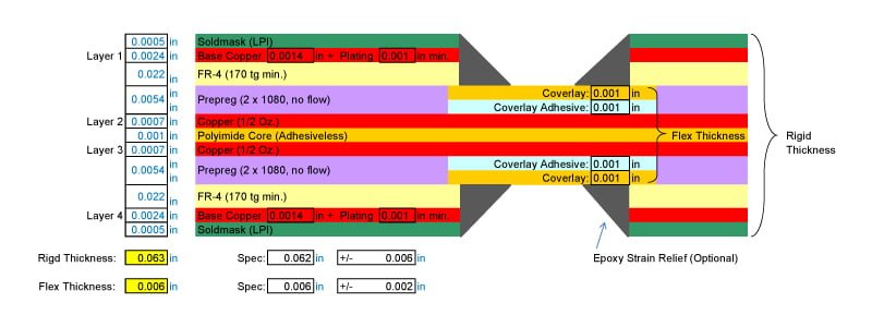
Optimizing High-Tg PCB Layer Stackup
High-Tg PCB layer stackup demands symmetry to mitigate warpage, a primary concern due to the material's thermal properties. Core and prepreg selections must match in Tg and resin content, with outer layers mirroring inner configurations. Place power and ground planes adjacent to signal layers for capacitance coupling and heat dissipation. Thinner dielectrics enable tighter impedance control while distributing thermal loads evenly. Engineers calculate stackup heights considering drill aspect ratios, as High-Tg resists breakthrough cleanly.
In multilayer High-Tg designs, alternate signal and plane layers to contain electromagnetic fields. Factory lamination presses benefit from controlled pressure ramps tailored to High-Tg's viscosity profile. Verify stackup via cross-section analysis post-build to confirm bondline thickness uniformity. Asymmetric builds invite bow and twist, compromising via reliability. This structured stackup fosters manufacturability and performance.
High-Tg PCB Via Design Strategies
High-Tg PCB via design prioritizes stub minimization and plating integrity, given the material's thermal expansion characteristics. Prefer blind and buried vias over through-holes to shorten signal paths and reduce inductance. Aspect ratios should stay below 10:1, accounting for High-Tg's stable drilling response. Implement staggered via patterns in dense areas to avoid heat buildup during sequential lamination. Post-plating inspection ensures void-free barrels, critical for High-Tg's higher modulus.
For high-density interconnects, microvias in High-Tg require laser drilling followed by plasma cleaning for optimal adhesion. Factory processes incorporate backdrilling to eliminate stubs in high-speed nets, preserving signal quality. Via tents and plugs protect against solder wicking during reflow. These choices align with performance specs in IPC-6012E, focusing on via reliability under thermal cycling. Thoughtful via placement enhances overall board yield.
Mastering High-Tg PCB Impedance Control
High-Tg PCB impedance control hinges on precise dielectric thickness and trace geometry within the stackup framework. Simulate characteristic impedance using field solvers, targeting 50 ohms single-ended or 100 ohms differential as common baselines. High-Tg prepregs offer consistent Dk values, but verify with TDR measurements on test coupons. Compensate for etch tolerances by widening traces slightly on inner layers. Factory fabs integrate impedance coupons per panel for inline verification.
Reference planes must remain unbroken under traces to stabilize return paths. In High-Tg designs, copper weight balancing prevents impedance drift from foil roughness. Length matching pairs with controlled lengths to avoid skew. These techniques ensure repeatable impedance across production runs. Engineers iterate stackups until simulations match fab capabilities.
Enhancing High-Tg PCB Signal Integrity
High-Tg PCB signal integrity benefits from the material's low loss at moderate frequencies, but design must address reflections and crosstalk. Route critical nets on inner layers sandwiched by planes, minimizing loop inductance. Use serpentine tuning for length equalization in high-speed buses. Avoid vias in tight bends to preserve waveform fidelity. Factory signal analysis confirms eye openings post-assembly.
Crosstalk mitigation involves increased spacing for adjacent high-speed traces, leveraging High-Tg's dimensional stability. Ground vias stitching planes tie returns effectively. Pre-layout planning identifies resonance risks from cavity effects in the stackup. These practices sustain clean signals through thermal excursions. Robust SI translates to fewer respins.
Manufacturing Best Practices for High-Tg PCBs
High-Tg PCB manufacturing thrives on controlled bake-out to remove moisture before lamination, preventing voids. Sequential buildup processes suit complex stackups, allowing intermediate inspections. Plasma desmear enhances via walls in High-Tg's tougher resin. Solder mask application demands UV-curable types for adhesion. Final bow/twist specs tighten to 0.75% max for High-Tg boards.
Incoming material verification confirms Tg via DSC testing per standards. Press cycles optimize dwell times for full flow without bleed-out. Electrical test fixtures account for High-Tg's planarity. These factory protocols yield high first-pass rates.
Conclusion
High-Tg PCB manufacturing hinges on integrated design tips spanning rules, stackup, vias, impedance, and signal integrity. Electrical engineers achieve optimal performance by prioritizing symmetry, simulation, and standard compliance. Factory-driven strategies ensure thermal resilience translates to reliable boards. Implementing these elements reduces risks in demanding applications. Future designs will lean further on High-Tg for evolving thermal challenges.
FAQs
Q1: What are essential High-Tg PCB design rules for multilayer boards?
A1: High-Tg PCB design rules focus on symmetric copper distribution, balanced drill aspect ratios under 10:1, and adequate annular rings to handle thermal stresses. Maintain consistent trace spacing to prevent shorts post-reflow. Factory alignment with IPC guidelines ensures manufacturability. These rules minimize warpage and enhance yield.
Q2: How does High-Tg PCB layer stackup impact impedance control?
A2: High-Tg PCB layer stackup influences impedance through dielectric spacing and plane proximity. Symmetric arrangements stabilize Dk uniformity for predictable 50-ohm traces. Inner signal layers between grounds reduce variations. Verify with coupons for production consistency.
Q3: Why is via design critical for High-Tg PCB signal integrity?
A3: High-Tg PCB via design affects signal integrity by controlling stubs and inductance. Blind vias shorten paths, while backdrilling clears resonances in high-speed nets. Proper plating prevents failures under heat. This preserves waveform quality in dense layouts.
Q4: What role does High-Tg play in overall PCB reliability?
A4: High-Tg materials boost reliability by resisting delamination and warpage in thermal cycles. Paired with optimized stackup and impedance, they support high-reliability apps. Factory processes like controlled lamination amplify benefits.
References
IPC-4101C — Specification for Base Materials for Rigid and Multilayer Printed Boards. IPC
IPC-2221 — Generic Standard on Printed Board Design. IPC
IPC-6012E — Qualification and Performance Specification for Rigid Printed Boards. IPC


