Introduction
High-speed digital circuits demand printed circuit boards that maintain signal integrity under demanding conditions. High-Tg PCB manufacturing addresses these needs by using materials with elevated glass transition temperatures, ensuring reliability in applications like telecommunications and computing systems. These boards resist deformation during thermal stresses from soldering or operation, which is critical for preserving electrical performance. Engineers specify High-Tg PCBs to minimize risks associated with standard materials that soften at lower temperatures. This article explores manufacturing processes, material properties, and best practices tailored for electric engineers designing high-speed systems. Factory insights reveal how precise control over production steps optimizes outcomes for complex circuits.
What Is a High-Tg PCB and Why It Matters for High-Speed Digital Circuits
A High-Tg PCB features laminates where the glass transition temperature exceeds typical FR-4 thresholds, providing superior thermal and mechanical stability. This property prevents excessive expansion or warpage during reflow soldering or high-power operation, common in high-speed digital designs. For electric engineers, the relevance lies in sustained electrical characteristics amid heat, avoiding signal degradation over time. Standard materials may shift properties above 150 degrees Celsius, compromising circuit reliability, while High-Tg variants maintain consistency. In high-speed contexts, this stability directly impacts data rates and error rates in routers or servers. Manufacturing these boards requires selecting resins that balance thermal resilience with electrical demands.
Industry demands for faster signals amplify the need for such materials, as thermal excursions from power dissipation intensify. High-Tg construction aligns with qualification under IPC-6012, ensuring boards meet performance specs for rigid printed boards. Engineers benefit from reduced rework in assembly, as these PCBs endure lead-free processes without delamination. Ultimately, specifying High-Tg elevates design margins in environments with thermal cycling.
Technical Principles of High-Tg Materials in High-Speed Applications
High-Tg PCB dielectric constant remains stable across temperature ranges, crucial for predictable signal propagation in digital circuits. Variations in dielectric constant alter propagation delay and crosstalk, disrupting timing in high-speed signals. Factory processes emphasize resin systems that minimize this variability, tested via standardized methods like those in IPC-TM-650. Engineers model circuits assuming consistent permittivity, so High-Tg materials support accurate simulations turning into reliable prototypes. Dissipation factor also plays a role, as elevated temperatures exacerbate losses in standard laminates.
High-Tg PCB signal loss stems primarily from dielectric absorption and conductor surface effects at frequencies above 1 GHz. Materials formulated for high Tg often incorporate fillers or curing agents that lower loss tangent without sacrificing thermal properties. In manufacturing, copper foil selection influences skin effect losses, where smoother profiles reduce attenuation. Engineers observe that controlled stacking sequences preserve low-loss paths through multilayer builds. Thermal stability prevents microcracks that could introduce intermittent losses during operation.
High-Tg PCB impedance matching relies on uniform dielectric thickness and consistent material properties throughout the board. Characteristic impedance formulas incorporate dielectric constant, so any gradient causes reflections and standing waves. Production involves precise control of prepreg flow and press cycles to achieve target thicknesses. For high-speed traces, differential pairs demand tolerances under 10 percent, achievable with High-Tg stacks. Vias and transitions further challenge matching, requiring back-drilling or filled techniques common in these builds.
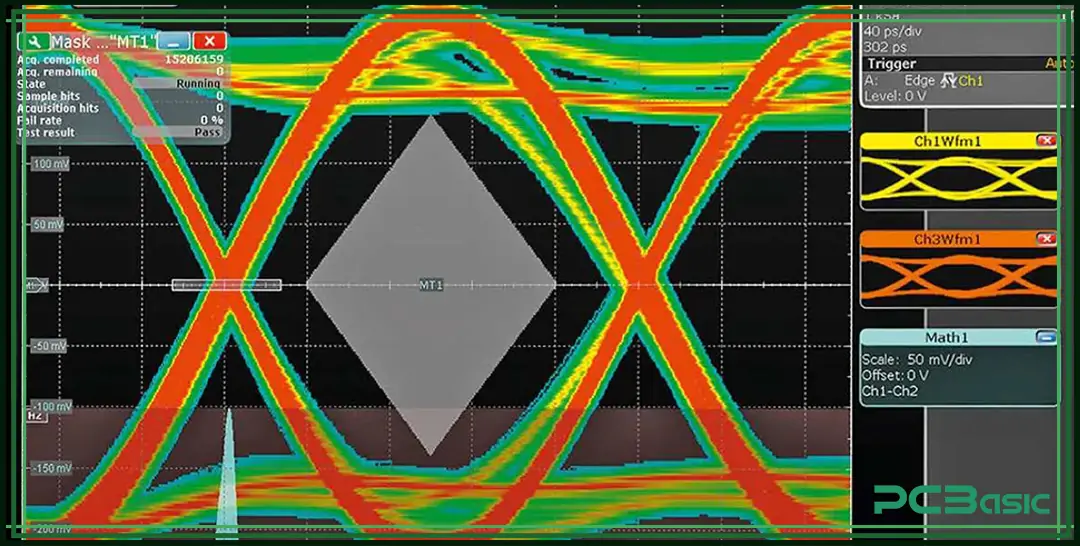
High-Tg PCB high-frequency performance excels due to reduced phase shift and group delay distortion. At multi-GHz bands, material anisotropy from glass weave can skew skew between traces, but High-Tg formulations mitigate this through tighter weave controls. Engineers prioritize low-roughness copper and thin dielectrics to extend usable bandwidth. Factory testing verifies performance via time-domain reflectometry, ensuring compliance before shipment.
Manufacturing Best Practices for High-Tg PCBs in High-Speed Designs
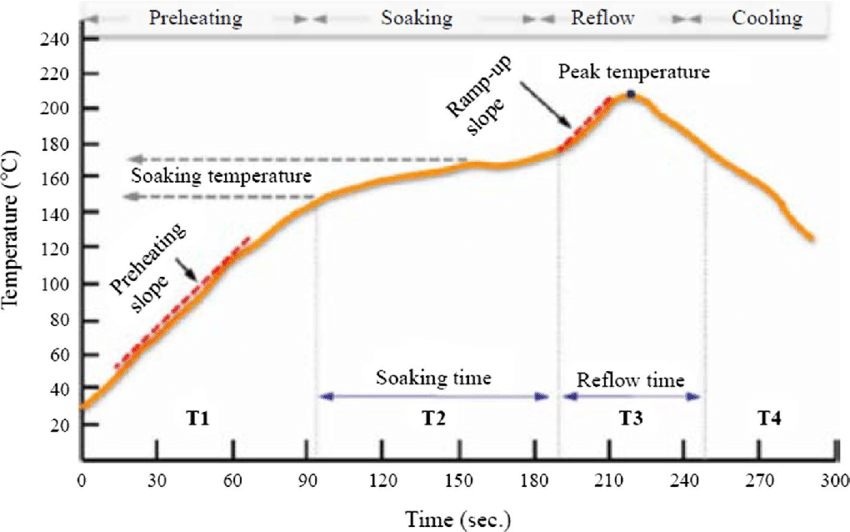
Material selection heads High-Tg PCB manufacturing, focusing on laminates meeting IPC-4101 specifications for base materials. Engineers specify grades with balanced CTE to match copper expansion, preventing barrel cracks in vias under thermal stress. Prepreg resin content must align with core for void-free lamination, achieved via vacuum pressing at optimized ramps. Factory protocols include dwell times exceeding standard cycles to fully cure high-Tg resins, enhancing interlayer adhesion.
Drilling and plating demand specialized parameters for High-Tg stacks, as harder resins resist standard bits. Entry and backup materials prevent burrs, while aspect ratios stay below 10:1 for reliable plating. Engineers request controlled depth drilling for blind vias, minimizing stubs that degrade high-speed signals. Post-plating anneals relieve stresses, improving ductility for subsequent processes.
Surface finishes like ENIG or soft gold suit high-speed needs, offering flat coplanarity for impedance-sensitive traces. High-Tg boards benefit from immersion tin for cost-effective oxidation resistance during storage. Solder mask application requires low-temperature cures to avoid Tg shifts, with photoimageable types preferred for fine-pitch features. Electrical testing includes impedance coupons at multiple points, correlating to High-Tg PCB impedance matching targets.
Routing and scoring use carbide tools with high flute counts to handle dense High-Tg boards without chipping. Beveling edges reduces stress risers in mechanical assemblies. Final bake stabilizes moisture before shipping, per JEDEC guidelines for handling. These steps ensure High-Tg PCB material for high-speed delivers as promised in field use.
Troubleshooting Common Issues in High-Tg PCB Production for High-Speed Circuits
Warpage emerges as a frequent challenge, traceable to CTE mismatches between layers. Engineers mitigate by symmetric stackups and constrained fixturing during lamination. Inspection via shadow moire confirms flatness post-process. CAF failures, or conductive anodic filamentation, arise from ionic residues in high-density vias; rigorous cleaning resolves this.
Signal anomalies post-assembly often link to plating voids affecting High-Tg PCB high-frequency performance. Cross-section analysis reveals coverage gaps, prompting adjusted current densities. Impedance drifts signal dielectric inconsistencies, addressed by refining prepreg ratios. Factory data logging trends these for process tweaks.
Conclusion
High-Tg PCB manufacturing equips high-speed digital circuits with thermal resilience and electrical precision. Stable dielectric properties curb signal loss and enable tight impedance matching, vital for gigabit data rates. Factory adherence to best practices, from material qual to final test, delivers boards ready for demanding deployments. Electric engineers gain confidence in designs pushing frequency limits without compromise. Selecting High-Tg elevates overall system reliability.
FAQs
Q1: What factors contribute to High-Tg PCB signal loss in high-speed applications?
A1: High-Tg PCB signal loss arises from dielectric dissipation and conductor losses at elevated frequencies. Material stability reduces temperature-induced increases in loss tangent, preserving eye openings. Manufacturing controls like low-roughness copper minimize skin effect contributions. Engineers verify via TDR measurements during qualification.
Q2: How does the High-Tg PCB dielectric constant affect impedance control?
A2: The High-Tg PCB dielectric constant determines transmission line velocity and characteristic impedance per standard equations. Consistent Dk across layers ensures matched pairs perform uniformly. Variations from poor lamination cause reflections, degrading signals. Factory processes target uniform resin distribution for reliable outcomes.
Q3: Why choose High-Tg PCB material for high-speed digital circuits?
A3: High-Tg PCB material for high-speed offers thermal endurance without degrading electrical specs. It withstands reflow peaks while keeping low signal attenuation. This suits multilayer builds with dense routing. Production aligns with IPC standards for proven quality.
Q4: What improves High-Tg PCB high-frequency performance during manufacturing?
A4: High-Tg PCB high-frequency performance benefits from thin dielectrics and symmetric stacks reducing modal dispersion. Precise drilling avoids via stubs impacting return loss. Controlled copper profiles lower insertion loss. Testing coupons confirm specs before assembly.
References
IPC-6012E — Qualification and Performance Specification for Rigid Printed Boards. IPC, 2017
IPC-4101E — Specification for Base Materials for Rigid and Multilayer Printed Boards. IPC, 2017
IPC-TM-650 — Test Methods Manual. IPC
JEDEC J-STD-020E — Moisture/Reflow Sensitivity Classification for Nonhermetic Surface Mount Devices. JEDEC, 2014


