What Is Via-in-Pad and Its Role in PCB Design?
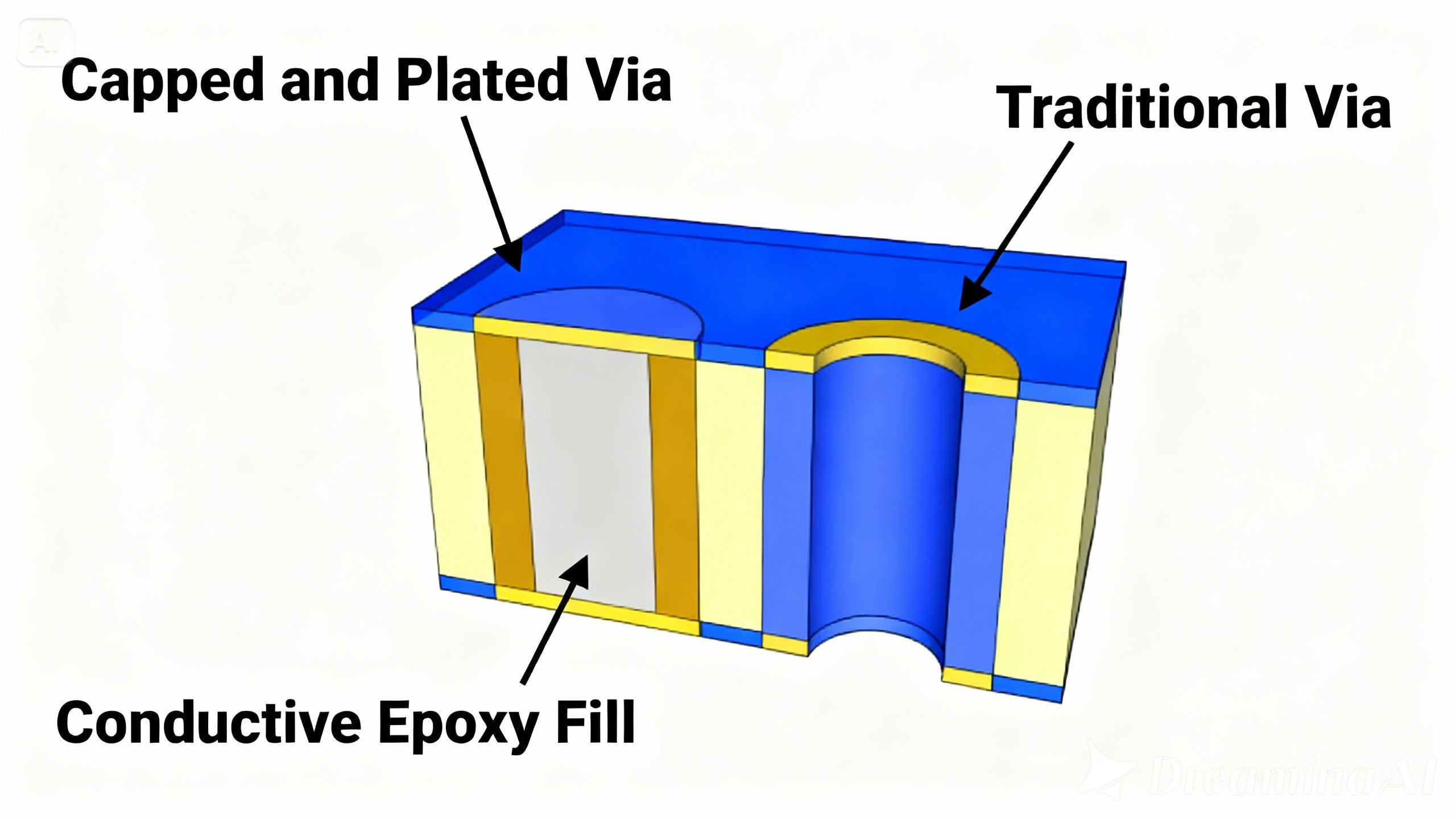
Via-in-pad is an advanced PCB design technique where a via—a small, plated hole connecting different layers of a circuit board—is positioned directly within a component's solder pad. This differs significantly from traditional vias, which are typically placed outside the pad area. The primary advantage of this method is its ability to conserve valuable board space, making it an ideal solution for compact, high-density electronic designs. This technology is widely adopted in modern consumer electronics, such as smartphones, tablets, and other miniaturized devices where maximizing board real estate is paramount.
While via-in-pad offers compelling benefits like enhanced signal integrity and reduced board size, its implementation invariably introduces higher manufacturing costs. These increased expenses are a direct result of the specialized processes required to successfully integrate this technology, particularly via filling and the use of high-density interconnect (HDI) manufacturing techniques. For engineers and designers, a thorough understanding of these cost drivers is essential to effectively balance performance goals with budgetary constraints.
Analyzing the Impact of Via-in-Pad on PCB Manufacturing Costs
The integration of via-in-pad technology has a direct and multifaceted influence on the overall cost of PCB manufacturing. This section delves into the primary factors that contribute to these elevated expenses, focusing on the costs associated with via filling, the complexities of HDI PCBs, and other related aspects that shape the total cost analysis for via-in-pad implementation.
The Cost of Via Filling
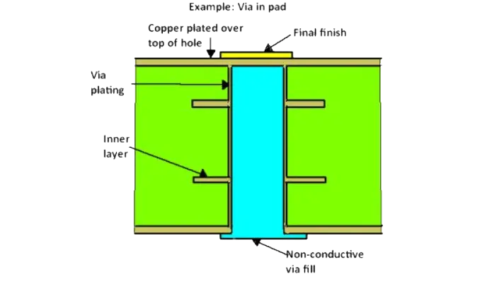
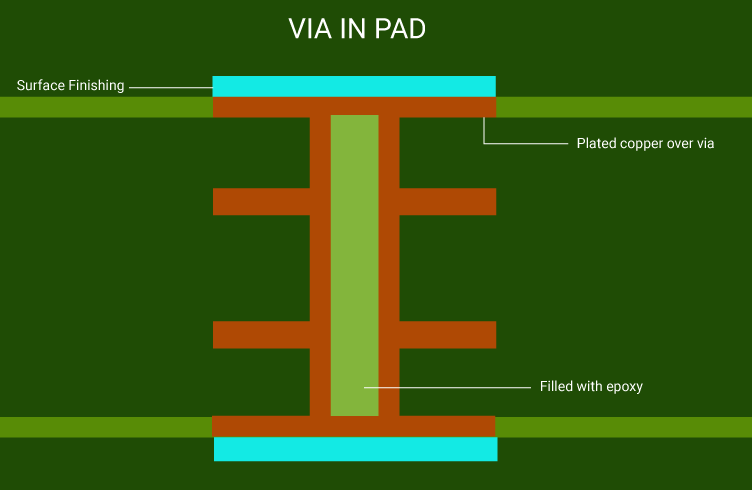
One of the most significant contributors to increased manufacturing costs with via-in-pad is the mandatory requirement for via filling. When a via is located directly within a component's pad, it can create issues during the soldering process, such as solder wicking down into the via barrel, which can compromise the integrity of the solder joint. To prevent these problems, the online PCB manufacturer must fill these vias with either a conductive or non-conductive material. This filling process adds both time and material expense to the production cycle.
Conductive filling, often utilizing copper, provides superior electrical and thermal performance but comes at a higher price due to the materials and precision involved. Non-conductive filling, typically done with epoxy, is a more economical option but still represents an additional cost compared to PCBs with unfilled, traditional vias. Depending on the board's specific requirements, the via filling process alone can escalate the total manufacturing cost of a via-in-pad PCB by anywhere from 10% to 30%. For instance, on a high-performance board featuring hundreds of via-in-pads, the cost per via for filling might range from $0.01 to $0.05. While seemingly small individually, this cost rapidly accumulates in large-scale production runs.
HDI PCB Complexity Drives Up Expenses
Via-in-pad technology is frequently employed in high-density interconnect (HDI) PCBs. These boards are specifically designed for compact, multilayer applications that feature finer traces and smaller vias (microvias). HDI manufacturing itself is inherently more expensive than standard PCB production due to the necessity of advanced equipment, stricter manufacturing tolerances, and additional lamination cycles. When via-in-pad is integrated into an HDI design, the costs escalate further. This is primarily due to the extreme precision required for aligning vias within pads and the specialized steps involved, such as laser drilling for microvias.
On average, HDI PCBs can command prices two to five times higher than conventional multilayer boards. For example, a standard 4 layer PCB board might cost around $0.50 per square inch, whereas an HDI board incorporating via-in-pad could range from $1.50 to $3.00 per square inch, depending on its complexity. This substantial increase in HDI PCB cost is a crucial consideration for any project planning to utilize via-in-pad technology.
Increased Design and Fabrication Complexity
Beyond the specific costs of via filling and HDI requirements, via-in-pad introduces additional layers of complexity to both the design and fabrication phases, further impacting the overall PCB manufacturing cost. Designers must meticulously account for tighter spacing constraints, ensure precise via placement, and proactively address potential signal integrity issues. These demands often necessitate the use of advanced design software and require the expertise of highly skilled engineers, potentially increasing design time and labor costs by 15% to 25% compared to more traditional PCB layouts.
During fabrication, manufacturers require specialized equipment capable of handling the stringent tolerances inherent in via-in-pad designs. For instance, laser drilling for microvias—a common feature in via-in-pad—is considerably more expensive than conventional mechanical drilling, often adding $0.10 to $0.20 per via. Furthermore, the heightened risk of manufacturing defects, such as misaligned vias or improper filling, can lead to board failures. This increases scrap rates and, consequently, the total production costs.
A Cost-Benefit Analysis of Via-in-Pad Technology
While the increased costs associated with via-in-pad are evident, conducting a thorough cost-benefit analysis is crucial to determine if its advantages genuinely outweigh the expenses for a specific project. This section explores the benefits and trade-offs to aid in informed decision-making.
Benefits That Justify the Investment
● Space Optimization: By integrating vias directly into component pads, the overall footprint of the PCB can be significantly reduced. This space-saving capability is paramount for miniaturized devices. While it may reduce material costs in some instances, this is often balanced by higher fabrication expenses.
● Enhanced Signal Integrity: Via-in-pad reduces the physical length of signal paths, thereby minimizing impedance mismatches. For high-speed designs operating at frequencies above 1 GHz, this can lead to substantial performance improvements, potentially avoiding costly redesigns later on.
● Superior Thermal Management: When conductive filling materials are used, via-in-pad technology can significantly improve heat dissipation. This is particularly vital for components like power integrated circuits (ICs) that generate considerable heat. Enhanced thermal management can extend the lifespan of the device, leading to savings in long-term maintenance and replacement costs.
Drawbacks and Key Cost Considerations
● Higher Initial Outlay: As previously discussed, the costs associated with via filling and the general complexity of HDI PCBs result in a higher initial financial investment. For projects with low production volumes, these increased upfront costs might not be justifiable.
● Manufacturing Complexities: The heightened risk of manufacturing defects combined with the necessity for specialized processes can lead to higher rejection rates, increasing material waste and the overall PCB manufacturing cost.
● Limited Manufacturer Options: Not all PCB fabricators possess the capabilities or expertise to handle complex via-in-pad designs, especially those involving HDI. This limitation can restrict your choice of suppliers, potentially leading to higher pricing due to reduced market competition.
Strategies for Managing Via-in-Pad Manufacturing Costs
Although via-in-pad inherently increases PCB manufacturing costs, several strategic approaches can help mitigate these expenses without compromising critical performance requirements.
Optimized Via Implementation
● Selective Use: Employ via-in-pad technology only where it provides clear advantages, such as for high-speed signal paths or in areas with extreme space constraints. For less critical components or signals, opt for traditional vias to reduce the associated via filling costs.
● Cost-Effective Filling: If the highest levels of thermal or electrical performance are not an absolute necessity, choose non-conductive epoxy filling over more expensive copper-based materials to achieve cost savings.
● Experienced Partners: Collaborate with PCB fabricators who possess proven expertise in both HDI and via-in-pad processes. This partnership can significantly minimize defects and rework, thereby reducing the overall PCB manufacturing cost.
● Balanced HDI Complexity: Avoid over-specifying the number of layers or the density of microvias in HDI designs. Simplifying the board's structure where feasible can lead to substantial reductions in HDI PCB cost.
Real-World Cost Implications
Examining real-world applications helps clarify the cost implications of via-in-pad. In the smartphone industry, for example, where board space is severely restricted, via-in-pad is frequently used to integrate more components into a smaller footprint. While the upfront manufacturing cost might be 20% higher than a traditional design, the ability to create a thinner, lighter, and more feature-rich device can significantly boost market competitiveness and sales, effectively offsetting the initial expense. Conversely, for applications like industrial control systems, where physical space is less of a critical constraint, the added cost of via-in-pad might not yield sufficient benefits. In such cases, a standard multilayer board with traditional vias could achieve the same functionality at a lower cost, making it a more economically sound choice.
Concluding Considerations: Is Via-in-Pad a Worthwhile Investment?
Via-in-pad technology undeniably leads to increased PCB manufacturing costs due to factors such as via filling expenses, the inherent complexity of HDI PCBs, and more demanding fabrication processes. However, the substantial benefits it offers—including significant space savings, improved signal integrity, and enhanced thermal management—can make it a highly valuable investment for designs that demand high performance and compact form factors. By thoroughly conducting a detailed cost-benefit analysis for your specific project and strategically applying cost-saving measures, you can achieve an optimal balance between budgetary constraints and critical performance objectives.


