Introduction
High-frequency PCB design demands precise control over signal integrity to support applications like RF PCB design and microwave PCB design. At frequencies above 1 GHz, signals propagate as transmission lines where mismatches in characteristic impedance lead to reflections, distorting waveforms and increasing signal loss. Impedance control ensures that traces maintain a consistent impedance, typically 50 ohms or 100 ohms differential, matching source and load requirements. This practice minimizes return loss and maximizes power transfer efficiency. Engineers must integrate impedance matching from the initial layout stage to avoid costly redesigns later in the development cycle.
Signal loss in high-frequency PCBs arises from multiple factors, including conductor resistance, dielectric absorption, and radiation. Without proper impedance control, these losses compound, degrading performance in radar systems, wireless communication, and high-speed data links. Adhering to established guidelines helps achieve low insertion loss and high signal fidelity. This article explores the principles, challenges, and best practices for implementing effective impedance control.
What Is Impedance Control and Why It Matters in High-Frequency PCBs
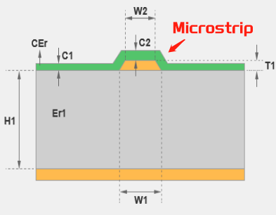
Impedance control refers to the process of designing and fabricating PCB traces to exhibit a predictable characteristic impedance, defined as the ratio of voltage to current for a traveling wave. In high-frequency PCB environments, this impedance remains constant along the transmission line, preventing reflections governed by the reflection coefficient formula. Common configurations include microstrip lines on outer layers and striplines embedded between planes. Achieving tolerances of ±10% or better requires coordination between design, material selection, and manufacturing processes.
The relevance of impedance control intensifies in RF PCB design and microwave PCB design, where wavelengths shorten to millimeters, making trace lengths electrically long. Mismatches cause standing waves, increasing voltage standing wave ratio (VSWR) and leading to signal loss through power reflected back to the source. According to IPC-6018D, qualification specifications for high-frequency printed boards emphasize tight impedance tolerances to ensure performance under operational conditions. Poor control results in bit error rates rising, reduced bandwidth, and compliance failures in telecommunications equipment.
Beyond reflections, signal loss manifests as attenuation, quantified in dB per unit length. Conductor losses dominate at lower high frequencies due to skin effect, confining current to the trace surface. Dielectric losses become prominent at microwave frequencies, proportional to the material's dissipation factor. Impedance mismatches exacerbate both by inducing mode conversions and crosstalk between adjacent traces.
Technical Principles of Impedance in High-Frequency Transmission Lines
Characteristic impedance derives from transmission line theory, approximated for PCBs as Z0 = sqrt(L/C), where L is inductance per unit length and C is capacitance per unit length. In microstrip structures, Z0 depends on trace width, dielectric height, and effective dielectric constant influenced by air above the trace. Striplines offer better control with symmetric dielectrics but require more layers. Coplanar waveguides provide field confinement for microwave PCB design, reducing radiation losses.
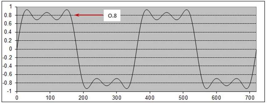
Reflections occur at discontinuities like vias, bends, or impedance steps, quantified by Γ = (Z_L - Z0)/(Z_L + Z0). Multiple reflections sum to distort the eye diagram, critical for high-speed signaling. Signal loss includes insertion loss from resistive and dielectric components, plus return loss from mismatches. At high frequencies, skin effect increases effective resistance as δ = sqrt(2/ωμσ), narrowing the current path.
Dielectric properties play a pivotal role, with permittivity (Dk) affecting velocity and loss tangent (Df) dictating energy dissipation. Materials must balance low Dk for high velocity and low Df for minimal attenuation. Conductor surface roughness further elevates losses by increasing effective path length. IPC-2141A provides guidelines for calculating these parameters in controlled impedance designs, ensuring predictions align with fabricated results.
Propagation delay, τ = sqrt(LC), ties directly to impedance, influencing timing budgets in synchronized systems. Engineers model these using field solvers to account for frequency-dependent effects. Understanding these principles enables proactive design to minimize signal loss.
Sources of Signal Loss and Their Relation to Impedance Control
Conductor loss stems from ohmic resistance, amplified by skin and proximity effects in dense routing. Rough copper surfaces scatter fields, adding up to several dB/m at 10 GHz. Impedance mismatches compound this by increasing current densities at reflection points. Smooth plating and wider traces mitigate these, but trade-offs with density arise.
Dielectric loss, α_d = (π f Dk Df)/c * sqrt(μ/ε), scales with frequency, demanding low-Df laminates for microwave applications. Variations in Dk homogeneity cause local impedance drifts, inducing differential mode conversions. Prepreg and core consistency during lamination proves essential.
Radiation loss occurs from unbalanced fields in asymmetric structures, minimized by ground plane proximity. Vias introduce stubs acting as resonators, peaking loss at quarter-wave frequencies. Backdrilling removes stubs, restoring impedance continuity. Crosstalk couples energy between aggressor and victim lines, worsened by impedance gradients.
Fabrication tolerances impact all losses: etch variation alters width, laminate thickness fluctuates height. Statistical process control targets ±0.1 mil etch and ±0.5 mil dielectric for high-frequency PCBs. These principles underscore impedance control's role in holistic signal integrity.
Practical Solutions and Best Practices for Impedance Control
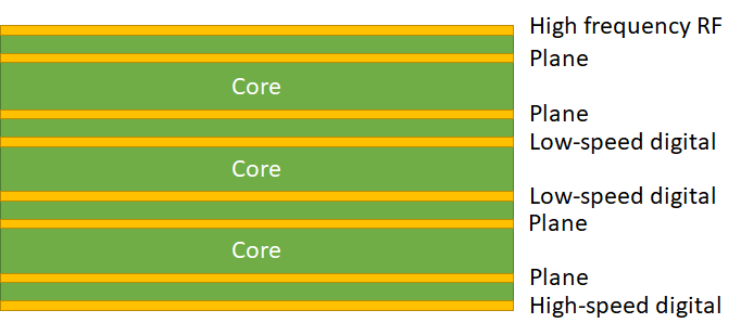
Effective impedance control begins with stackup design, optimizing layer count, dielectric thicknesses, and plane assignments. Symmetric builds prevent warpage, maintaining uniform heights. Reference planes adjacent to signal layers cap fields, stabilizing Z0. Simulate stackups to predict impedance across frequencies.
Trace geometry demands precise width and spacing calculations using Wheeler or Hammerstad equations from IPC-2141A. Target 50-ohm single-ended or 100-ohm differential, verifying with 2D/3D solvers. Etch compensation accounts for under-etch in inner layers. Routed slots or filled vias preserve continuity.
Material selection favors low-loss dielectrics with stable Dk/Df up to 40 GHz. Hybrid stacks combine FR-4 cores with high-frequency skins for cost-performance balance. Thermal expansion matching avoids stress-induced drifts. IPC-TM-650 test methods, such as 2.5.5.7 for TDR, validate fabricated impedances.
Via design minimizes transitions: blind/buried vias reduce stub length, tapered profiles smooth impedance steps. Stitching vias along reference edges return currents efficiently. Length-matched routing preserves phase alignment in differential pairs.
Layout practices include 45-degree bends over 90-degree for smooth transitions, minimizing radiation. Guard traces shield sensitive lines. Power integrity couples with signal, as plane resonances interact.
Testing integrates flying probe TDR during fab and VNA S-parameters post-assembly. Tolerance specs like ±10% single-ended, ±5% differential ensure margins. Iterative feedback refines processes.
Troubleshooting Common Impedance-Related Issues
Engineers often encounter impedance drifts from fabrication variances, diagnosed via TDR ripples. Cross-section analysis reveals etch or height errors. Adjust artwork scaling accordingly.
Via stubs cause resonant nulls in frequency response; model stub length and backdrill if exceeding 1/10 wavelength. Differential skew from unequal lengths amplifies common-mode noise.
Crosstalk spikes indicate inadequate spacing; increase gap or add ground traces. Signal loss plateaus suggest dielectric issues; measure Df via split-post resonators.
Post-layout simulation flags violations early. Prototype validation confirms models.
Conclusion
Impedance control forms the cornerstone of high-frequency PCB design, directly combating signal loss through reflection mitigation and loss reduction. From transmission line fundamentals to fabrication tolerances, every step influences performance in RF and microwave applications. Best practices like precise stackups, low-loss materials, and rigorous testing yield reliable boards. Engineers applying these structured approaches achieve superior signal integrity, meeting demanding specs efficiently.
FAQs
Q1: What role does impedance matching play in minimizing signal loss in high-frequency PCBs?
A1: Impedance matching ensures transmission lines match source and load impedances, preventing reflections that cause return loss. In RF PCB design, mismatches elevate VSWR, dissipating power as heat. Proper matching, via controlled trace geometries, preserves waveform integrity and reduces attenuation. Tolerances under ±10% maintain low signal loss across GHz bands.
Q2: How do you achieve controlled impedance in microwave PCB design?
A2: Design stackups with consistent dielectric thicknesses and reference planes to stabilize Z0. Calculate trace widths using guidelines from standards like IPC-2141A for microstrip or stripline. Select materials with low Df to curb dielectric losses. Verify with TDR testing per IPC-TM-650 methods during fabrication. This systematic approach minimizes signal loss effectively.
Q3: What are the primary causes of signal loss in high-frequency PCBs despite impedance control?
A3: Conductor losses from skin effect and roughness, plus dielectric absorption via Df, dominate. Vias and discontinuities induce mismatches, amplifying reflections. Radiation from unbalanced fields adds marginally. Mitigate with smooth copper, backdrilling, and symmetric layouts to complement impedance matching.
Q4: Why is stackup design critical for impedance control and signal integrity?
A4: Stackups define dielectric heights and plane proximity, directly dictating capacitance and thus Z0. Uniform builds prevent warpage-induced drifts. Hybrid materials optimize loss profiles for microwave frequencies. Simulations predict performance, guiding iterations to minimize signal loss in high-frequency applications.
References
IPC-2141A — Design Guide for High-Speed Controlled Impedance Circuit Boards. IPC, 2004
IPC-6018D — Qualification and Performance Specification for High Frequency (Microwave) Printed Boards. IPC
IPC-TM-650 2.5.5.7 — Characteristic Impedance of Lines on Printed Boards by TDR. IPC


