Introduction
In modern electronics, high-speed signals demand precise control over transmission line characteristics to ensure reliable performance. Impedance-controlled PCB manufacturing addresses this need by maintaining consistent characteristic impedance across traces, minimizing signal reflections and distortion. However, achieving this control introduces significant PCB impedance control challenges during both design and fabrication phases. Engineers must navigate variations in materials, processes, and geometries that can deviate impedance from target values. PCB layer stackup issues and PCB material properties impact play critical roles, often leading to signal integrity problems if not managed properly. This article explores these hurdles and provides factory-driven strategies aligned with industry standards to overcome them effectively.
As signal frequencies rise in applications like telecommunications and data centers, even minor impedance mismatches can cause crosstalk, attenuation, or timing errors. Fabrication tolerances further complicate matters, requiring tight process controls to meet specifications. Designers and manufacturers collaborate closely to specify stackups and materials that support controlled impedance. Understanding these interactions allows teams to produce boards that perform reliably under real-world conditions. By focusing on proven practices, electrical engineers can mitigate risks and enhance product quality.
What Is Impedance Control in PCBs and Why It Matters
Impedance control refers to the process of designing and fabricating printed circuit boards where the characteristic impedance of signal traces matches specified values, typically for high-speed applications. Characteristic impedance arises from the interaction between trace geometry and surrounding dielectric materials, governed by transmission line theory. In uncontrolled boards, random variations lead to reflections that degrade signals, but controlled impedance ensures predictable propagation. This is essential for maintaining signal integrity in differential pairs, single-ended lines, and RF circuits.
The relevance grows with increasing data rates, where even small deviations amplify errors. For instance, in multilayer boards, impedance mismatches at vias or layer transitions exacerbate issues. Industry standards like IPC-2141A provide guidelines for designing these structures, emphasizing test coupons and calculation methods. Without proper control, boards fail compliance tests or field performance, leading to costly redesigns. Thus, impedance control directly impacts yield, reliability, and time-to-market for electrical engineers.
Key Technical Principles of Impedance Control
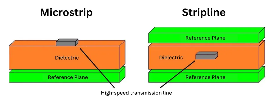
Characteristic impedance in PCBs follows principles from electromagnetic theory, where Z0 equals sqrt(L/C) for inductance L and capacitance C per unit length. For microstrip lines, exposed to air and dielectric, impedance depends on trace width, height above reference plane, and effective dielectric constant. Striplines, embedded between planes, rely more heavily on dielectric thickness uniformity. Variations in any parameter shift Z0, necessitating precise modeling during design.
Material properties fundamentally influence these calculations, as dielectric constant Er dictates capacitance. Factory lamination processes must achieve consistent prepreg and core thicknesses to match design assumptions. Copper etching defines trace width, while plating adds thickness that alters effective geometry. Engineers use field solvers or empirical formulas from standards to predict values, but real-world fabrication introduces discrepancies. Balancing these factors ensures traces meet target impedances across the board.
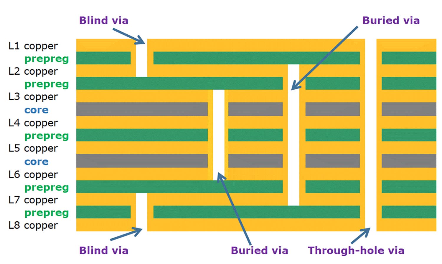
PCB Impedance Control Challenges in Design
Design phase PCB impedance control challenges stem primarily from PCB layer stackup issues, where layer thicknesses and material sequencing affect field distribution. Asymmetric stackups can cause unintended coupling or resonance, complicating impedance matching. Engineers must iterate stackups to optimize for both impedance and manufacturability, considering drill aspect ratios and via stub effects. Simulations help predict behavior, but assumptions about material Er often prove optimistic due to supplier variations.
PCB material properties impact further heightens these challenges, as dielectric constants vary with frequency, temperature, and resin content. Low-loss materials for high-speed designs introduce higher costs and tighter thickness controls. Selecting cores and prepregs requires data sheets aligned with stackup needs, yet batch-to-batch inconsistencies persist. Designers specify net classes with target Z0 and tolerances, but without factory feedback, revisions multiply. Proactive stackup planning mitigates these risks, ensuring design rules support fabrication feasibility.
Manufacturing Challenges: Controlled Impedance Manufacturing Tolerances
During fabrication, controlled impedance manufacturing tolerances become paramount, as processes like lamination, etching, and plating introduce variations. Dielectric thickness can fluctuate from press cycles, altering capacitance and thus Z0. Copper plating buildup narrows effective trace width, demanding compensation in artwork. Etch factor, influenced by chemistry and panel size, skews dimensions across large boards. Factories implement statistical process control to hold tolerances, but multilayer alignment adds complexity.
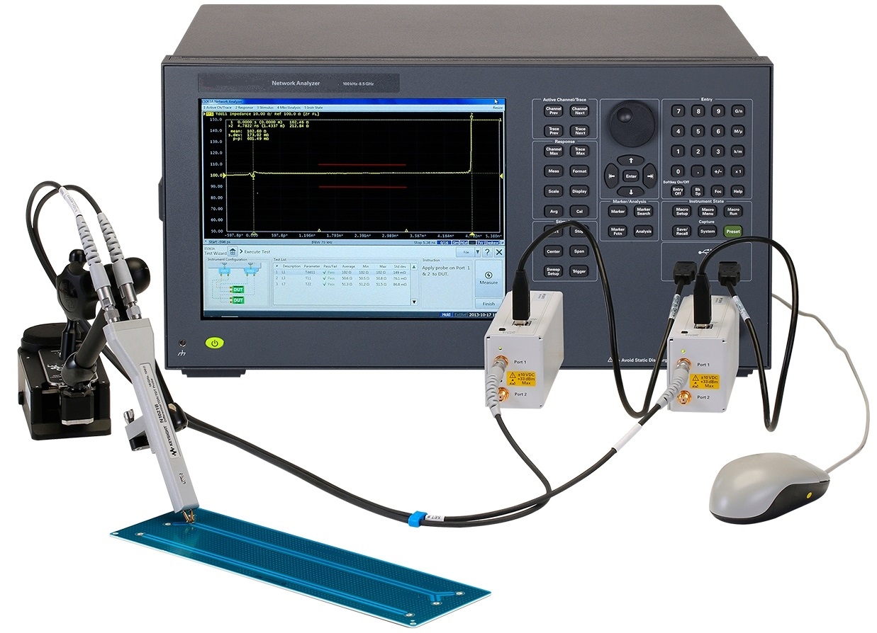
PCB material properties impact manifests in absorption during lamination, causing shrinkage or warpage that misaligns layers. High Tg materials resist this but demand precise cure cycles. Impedance test coupons, placed at board edges per IPC-2141A, verify compliance using time-domain reflectometry. Deviations trigger rework or scrap, underscoring the need for upfront material qualification. Tight fab controls, including automated optical inspection, bridge design intent to production reality.
Best Practices for Overcoming Design and Fabrication Challenges
To address PCB layer stackup issues, engineers start with symmetric constructions, alternating signal and plane layers for balanced fields. Collaborate with fabricators early to validate stackup using their material library and press capabilities. Specify minimum dielectric spacing and use blind vias to shorten stubs. Simulations incorporating fab tolerances predict worst-case Z0 shifts, guiding adjustments.
For controlled impedance manufacturing tolerances, factories employ dedicated impedance lines in panels for inline testing. Select low-variation prepregs and control lamination pressure uniformly. Post-etch plating processes use pulse techniques to minimize buildup. IPC-6012E outlines performance specs, including impedance verification for qualified boards. Document all parameters in traveler sheets for traceability.
Material selection counters PCB material properties impact by prioritizing consistent Er materials with low loss tangents. Qualify lots via DK/Df testing before commitment. Hybrid stackups blending high-speed and standard layers optimize cost without compromising control.
Troubleshooting Insights from Factory Experience
Common PCB impedance control challenges appear as TDR waveforms showing steps or ringing, often from stackup asymmetry. Verify coupon locations avoid warpage-prone edges. If plating shifts Z0 high, reduce current density; low shifts indicate over-etch. Layer registration issues cause crosstalk; X-ray confirms alignment.
For persistent deviations, audit material certificates against incoming specs. Thermal profiling during lamination prevents voids affecting thickness. Post-fab baking stabilizes dimensions before testing. These factory-driven steps, aligned with standards, resolve most issues without full respins.
Conclusion
Impedance-controlled PCB manufacturing demands vigilance across design and fabrication to conquer inherent challenges. PCB impedance control challenges, PCB layer stackup issues, controlled impedance manufacturing tolerances, and PCB material properties impact interlink, requiring integrated approaches. Leveraging standards like IPC-2141A and IPC-6012E ensures compliance and performance. Electrical engineers benefit from early collaboration, precise modeling, and process rigor. Implementing these practices yields reliable high-speed boards, advancing electronics innovation.
FAQs
Q1: What are the main PCB impedance control challenges in high-speed designs?
A1: PCB impedance control challenges arise from variations in trace geometry, dielectric properties, and process tolerances that cause signal reflections. Stackup asymmetries and material inconsistencies amplify mismatches, leading to crosstalk or attenuation. Engineers mitigate this through simulations and test coupons, ensuring Z0 stays within specs. Factory validation confirms design intent.
Q2: How do PCB layer stackup issues impact impedance control?
A2: PCB layer stackup issues disrupt field uniformity, altering capacitance and inductance for signal traces. Asymmetric planes cause unintended coupling, while thickness variations shift Z0. Balanced designs with reference planes resolve this, supported by fab feedback. Proper sequencing prevents warpage, maintaining tolerances throughout manufacturing.
Q3: What role does PCB material properties impact play in controlled impedance?
A3: PCB material properties impact impedance via dielectric constant Er fluctuations, affecting capacitance directly. Resin content and thickness variations from lamination alter effective Z0. Low-loss materials with stable properties minimize deviations, qualified per standards. Consistent selection ensures predictable performance in high-frequency applications.
Q4: How are controlled impedance manufacturing tolerances managed in production?
A4: Controlled impedance manufacturing tolerances demand tight process controls in etching, plating, and lamination to hold Z0 variations low. Inline TDR testing on coupons verifies compliance. Statistical monitoring and material qualification align fab capabilities with design specs, reducing scrap and rework effectively.
FAQs
IPC-2141A — Design Guide for High-Speed Controlled Impedance Printed Boards. IPC, 2007
IPC-6012E — Qualification and Performance Specification for Rigid Printed Boards. IPC, 2017
IPC-A-600K — Acceptability of Printed Boards. IPC, 2020


