Introduction
Printed Circuit Boards (PCBs) form the backbone of modern electronics, supporting critical applications in industries like aerospace, automotive, and telecommunications. Ensuring their reliability under diverse operating conditions is essential for preventing failures and extending product life. Highly Accelerated Life Testing (HALT) and Highly Accelerated Stress Screening (HASS) are proven methodologies for enhancing PCB design by identifying weaknesses early and improving robustness. These accelerated testing approaches simulate extreme conditions to uncover potential PCB failure points, allowing engineers to address issues before they impact end users. By integrating HALT and HASS into the design and production phases, manufacturers can boost product life span and ensure consistent performance. This article explores the technical foundations of these methods, their application in PCB design, and practical strategies for implementation, tailored for electrical engineers seeking to optimize reliability.
What Are HALT and HASS, and Why Do They Matter
HALT and HASS are specialized testing methodologies aimed at improving product reliability through accelerated stress testing. HALT focuses on the design phase, subjecting prototypes to extreme environmental conditions such as temperature, vibration, and thermal cycling to identify design flaws. The goal is to push components beyond their operational limits to reveal weak points that could lead to PCB failure in real-world scenarios. HASS, on the other hand, is applied during production to screen out manufacturing defects in finished products, ensuring only robust units reach the market.
These methods matter because they directly impact the robustness and life span of PCBs. Traditional testing often fails to simulate the harsh conditions products may encounter over time. Accelerated testing with HALT and HASS bridges this gap, enabling engineers to predict and mitigate failures, reduce warranty costs, and build trust in their designs. For industries where downtime is costly, these approaches are indispensable for maintaining quality and performance.
Technical Principles of HALT and HASS in PCB Testing
Understanding HALT Mechanics
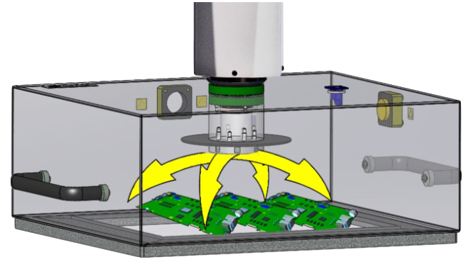
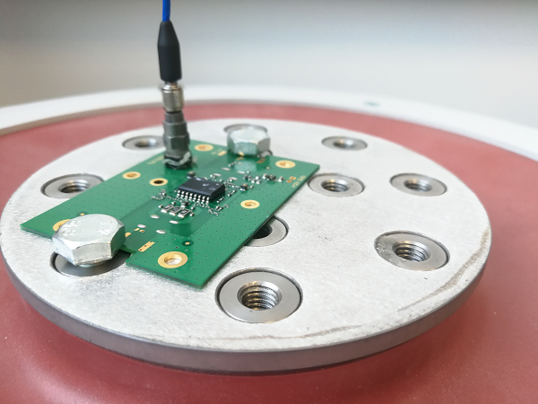
HALT involves exposing the quick PCB prototype to a combination of environmental stresses, typically including rapid temperature changes, vibration, and power cycling. The process is governed by standards such as JEDEC JESD22-A110E, which outlines test conditions for evaluating electronic component reliability under stress. Temperature extremes often range beyond typical operating limits to force failures, revealing design vulnerabilities. Vibration testing simulates mechanical stress, identifying issues like solder joint fatigue or component detachment. The iterative nature of HALT means that once a failure is detected, designers refine the PCB layout or materials and retest until robustness improves.
HASS Application in Production
HASS builds on HALT findings by applying less severe but still accelerated stress conditions to production units. It uses predefined stress profiles based on HALT results to detect manufacturing inconsistencies, such as poor soldering or defective components. HASS aligns with guidelines like IPC-9592A, which provides frameworks for reliability testing of electronic hardware. By screening out defective units before shipment, HASS ensures that only PCBs meeting robustness criteria reach customers, directly contributing to a longer product life span.
Stress Factors and Failure Modes
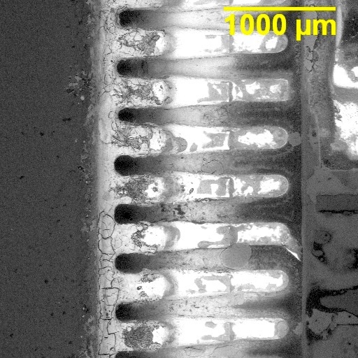
Both methods target common PCB failure modes, including thermal expansion mismatches, mechanical fatigue, and electrical overstress. Thermal cycling, for instance, can cause warpage or delamination if materials are not properly matched, as outlined in IPC-6012E for rigid PCB performance specifications. Vibration stress often exposes weaknesses in mounting or interconnects, while electrical stress tests uncover issues like insulation breakdown. Understanding these failure mechanisms through accelerated testing allows engineers to design PCBs that withstand real-world challenges.
Benefits of HALT and HASS for PCB Design
Early Detection of Design Flaws
HALT identifies potential issues during the design phase, long before production begins. By simulating extreme conditions, it reveals weaknesses that might not surface in standard testing, enabling engineers to modify layouts, select more durable materials, or adjust component placement. This proactive approach minimizes the risk of PCB failure in the field and reduces costly redesigns.
Enhanced Product Robustness
The iterative feedback from HALT and HASS drives continuous improvement in PCB robustness. For example, addressing a solder joint failure identified in HALT by optimizing reflow profiles or pad designs ensures the quick turn PCB can endure mechanical stress. Robustness directly correlates with a longer life span, as the board becomes less susceptible to environmental or operational stressors.
Cost and Time Efficiency
While accelerated testing requires upfront investment, it saves significant costs by preventing field failures and warranty claims. HASS, in particular, streamlines production quality control by quickly identifying defective units. According to industry practices aligned with ISO 9001:2015 for quality management, integrating such testing reduces long-term expenses and accelerates time to market by catching issues early.
Practical Implementation of HALT and HASS in PCB Design
Setting Up HALT for Design Validation
To implement HALT, engineers must first define the operational limits of the PCB based on its intended application. Test chambers capable of extreme temperature transitions and vibration are essential. The process begins with incremental stress application, monitoring for failures like cracks or electrical shorts. Each failure prompts a root cause analysis, followed by design adjustments. Standards such as JEDEC JESD22-A110E provide detailed protocols for setting stress levels and durations, ensuring consistency in testing.
Developing HASS for Production Screening
HASS requires a tailored stress profile derived from HALT data, focusing on manufacturing defects rather than design flaws. Engineers should establish test parameters that balance effectiveness with production throughput. IPC-9592A offers guidance on acceptable stress screening levels for electronic assemblies, ensuring that HASS does not damage good units while still catching defects. Automated test setups can enhance efficiency, logging results for quality assurance.
Key Considerations for Engineers
When applying these methods, consider the following best practices. First, ensure material compatibility with expected stress levels, referencing IPC-6012E for performance criteria. Second, prioritize failure analysis to understand root causes, using techniques like microscopic inspection for solder joints. Third, maintain detailed documentation of test conditions and outcomes to comply with ISO 9001:2015 quality standards. Finally, integrate findings into design rules to prevent recurring issues, enhancing overall PCB reliability.
 bbbbbbb
Integrating HALT and HASS into the Design Workflow
Collaboration Across Teams
Effective use of accelerated testing requires collaboration between design, manufacturing, and quality control teams. Designers must share HALT results to inform material selection and layout rules, while manufacturing teams use HASS data to refine assembly processes. Regular cross-functional reviews ensure that insights from testing translate into actionable improvements, aligning with quality management principles in ISO 9001:2015.
Iterative Design Improvements
HALT and HASS foster an iterative approach to PCB design. Each test cycle provides data to refine board layouts, component choices, and manufacturing techniques. For instance, discovering a thermal stress failure might lead to selecting materials with better coefficients of thermal expansion, as specified in IPC-6012E. This continuous feedback loop builds robustness over time, extending the PCB life span.
Monitoring Long-Term Impact
Beyond initial testing, engineers should track field performance to validate HALT and HASS predictions. Collecting data on failure rates and environmental exposure helps refine test profiles for future designs. This long-term monitoring aligns with reliability engineering practices outlined in IPC-9592A, ensuring that accelerated testing remains relevant to real-world conditions.
Challenges and Limitations of HALT and HASS
Resource Intensity
Implementing HALT and HASS requires specialized equipment and trained personnel, which can strain budgets and timelines. Small design teams may struggle to allocate resources for comprehensive testing, limiting the scope of stress conditions applied. Planning and prioritization are crucial to balance cost with reliability goals.
Risk of Overstress
Excessive stress during HALT can sometimes induce failures that would never occur in normal use, leading to unnecessary design changes. Engineers must carefully calibrate test conditions, adhering to standards like JEDEC JESD22-A110E, to ensure results reflect realistic failure modes. HASS also risks damaging functional units if stress levels are not properly controlled.
Interpretation of Results
Analyzing test data requires expertise to distinguish between design flaws, manufacturing defects, and test-induced artifacts. Misinterpretation can lead to incorrect solutions, undermining robustness. Thorough documentation and adherence to protocols in IPC-9592A help ensure accurate conclusions from accelerated testing.
Conclusion
HALT and HASS offer powerful tools for improving PCB design by identifying weaknesses through accelerated testing. These methodologies enhance robustness, prevent PCB failure, and extend product life span by simulating extreme conditions and screening for defects. By understanding the technical principles behind HALT and HASS, electrical engineers can integrate these practices into their workflows, ensuring reliable performance in demanding applications. Practical implementation, supported by industry standards, allows for early flaw detection and iterative design improvements. While challenges like resource demands and data interpretation exist, the benefits of reduced field failures and improved quality far outweigh the hurdles. Embracing these testing strategies is a critical step toward building durable, high-performing PCBs.
FAQs
Q1: How does HALT improve PCB robustness during the design phase?
A1: HALT improves PCB robustness by subjecting prototypes to extreme environmental stresses like temperature and vibration. This accelerated testing reveals design weaknesses early, allowing engineers to refine layouts or materials before production. Following standards like JEDEC JESD22-A110E ensures consistent stress application. By addressing issues proactively, HALT ensures the PCB can withstand real-world conditions, reducing the likelihood of failures.
Q2: What role does HASS play in preventing PCB failure in production?
A2: HASS plays a vital role in preventing PCB failure by screening production units for manufacturing defects. Using stress profiles derived from HALT, it identifies issues like poor soldering under accelerated conditions. Guided by IPC-9592A, HASS ensures only robust units reach the market. This process minimizes field failures, maintaining product reliability and customer satisfaction.
Q3: How does accelerated testing impact the life span of a PCB?
A3: Accelerated testing, through HALT and HASS, significantly enhances PCB life span by identifying and mitigating potential failure points early. HALT uncovers design flaws, while HASS catches production defects, ensuring durability. By simulating harsh conditions as per JEDEC JESD22-A110E, these methods predict long-term performance. The result is a PCB better equipped to endure operational stresses over time.
Q4: What standards guide the implementation of HALT and HASS for PCB testing?
A4: HALT and HASS implementation for PCB testing is guided by standards like JEDEC JESD22-A110E for stress test conditions and IPC-9592A for reliability screening protocols. IPC-6012E provides performance specifications for rigid PCBs, ensuring material and design compatibility. ISO 9001:2015 supports quality management during testing. These standards ensure consistent, reliable results across testing phases.
References
JEDEC JESD22-A110E — Highly Accelerated Temperature and Humidity Stress Test (HAST). JEDEC, 2015.
IPC-9592A — Requirements for Power Conversion Devices for the Computer and Telecommunications Industries. IPC, 2010.
IPC-6012E — Qualification and Performance Specification for Rigid Printed Boards. IPC, 2020.
ISO 9001:2015 — Quality Management Systems. ISO, 2015.


