Introduction
In-circuit testing stands as a cornerstone in printed circuit board assembly quality control, verifying component values, solder joint integrity, and electrical connectivity on fully populated boards. Dual-site testing elevates this process by enabling parallel testing of two boards simultaneously within a single fixture, optimizing production workflows in high-volume manufacturing environments. This approach aligns with factory demands for efficiency while upholding rigorous quality standards. Electric engineers appreciate how dual-site configurations address throughput bottlenecks without compromising test depth. As production scales, integrating such methods becomes essential for maintaining competitive edges in PCB assembly lines.
What Is In-Circuit Testing with Dual-Site Test?
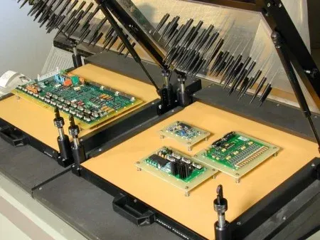
In-circuit testing, or ICT, employs a bed-of-nails fixture to make electrical contact with numerous test points on a PCB assembly, allowing measurements of resistors, capacitors, diodes, and shorts or opens across nets. Dual-site ICT extends this by incorporating two independent test areas into one fixture, where probes contact points on both boards at once, and the tester executes identical test programs in parallel. This multi-site architecture supports scalability, permitting expansion to four or more sites as production volumes grow. Factory engineers design these systems to handle identical board variants, ensuring consistent fault detection rates. The method matters because it directly impacts yield rates and time-to-market in demanding sectors like automotive and consumer electronics.
Parallel testing in dual-site setups halves the effective test cycle time per board compared to single-site operation. Reliability remains paramount, as fixtures must prevent electrical crosstalk between sites through precise guarding and shielding techniques. Engineers specify test points during PCB layout to facilitate such probing, adhering to established guidelines for accessibility.
Technical Principles of Dual-Site In-Circuit Testing
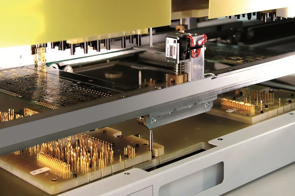
The core of dual-site ICT lies in the bed-of-nails fixture, a mechanical interface with spring-loaded probes aligned to PCB test points via precision-machined tooling plates. Each site features its own array of probes, often numbering in the thousands, connected to multiplexers that route signals to shared or dedicated instrumentation channels for parametric measurements. Parallel testing occurs as the system applies stimuli independently to each site, measuring direct current resistance, capacitance, and component orientation while isolating sites with guard nets to minimize interference. This multi-site architecture demands careful pin assignment to avoid shared ground loops or capacitive coupling between boards.
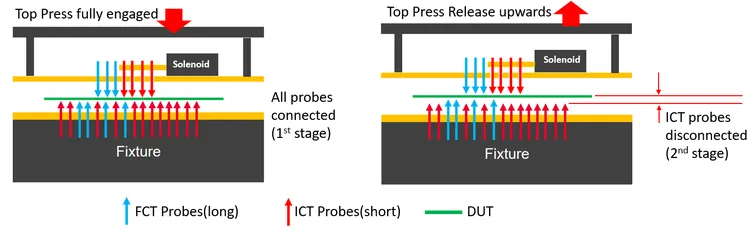
Fixture design incorporates alignment pins and pneumatic presses for repeatable contact force, typically 50 to 150 grams per probe, ensuring low-resistance connections under 20 milliohms. Software sequences tests site-by-site or simultaneously, logging results for each board uniquely to support traceability. Electric engineers focus on Kelvin four-wire sensing for high-accuracy voltage and current measurements, critical for verifying low-value components. Compliance with standards like IPC-9252 for electrical test fixturing principles guides probe spacing and density to achieve reliable contacts.
In operation, the tester powers down unprotected nets to safeguard active components, applying guarding voltages to float sensitive nodes. Dual-site systems scale by modular instrumentation, where channel counts double without proportional cost increases. This setup enhances factory throughput while preserving the granularity of single-site diagnostics.
Benefits of Parallel Testing and Scalability
Parallel testing in dual-site ICT directly boosts production efficiency by processing two assemblies per fixture cycle, effectively doubling output without duplicating full tester hardware. Scalability shines in multi-site architecture, where fixtures evolve from dual to quad sites, accommodating rising volumes through incremental investments in probes and channels rather than entire systems. This modularity reduces costs by amortizing fixture development and maintenance over more units tested.
Accuracy and reliability hold steady, as each site mirrors single-site probing fidelity when designed with site isolation. Factories report consistent fault coverage above 95 percent for opens, shorts, and wrong-value components across sites. Cost reductions stem from lower per-board test times, minimizing labor and equipment depreciation in high-mix, medium-volume runs.

Engineers value how this approach integrates with automated handling, feeding boards into fixtures via robotic loaders for unmanned operation. Overall, it transforms testing from a bottleneck into a scalable asset.
Implementing Dual-Site Test Fixtures: Best Practices
Successful dual-site implementation starts with PCB design for testability, placing accessible vias or pads at every net, spaced at least 0.050 inches apart to accommodate probe diameters. Factory teams collaborate early, simulating fixture layouts to optimize probe lengths and angles, avoiding mechanical interference between sites. J-STD-001 requirements for soldered assemblies inform test limits, ensuring ICT verifies joint integrity without false calls.
Fixture fabrication uses high-precision CNC machining for top and bottom plates, with wire-wrap or etched wiring to channels exhibiting less than 1 ohm resistance. Engineers program test sequences prioritizing high-failure nets first, incorporating self-learn routines to baseline golden boards per site. Regular calibration maintains probe integrity, with automated pressure checks preventing weak contacts.
To enhance accuracy and reliability, incorporate active guarding where adjacent probes on different sites share no common signals. Multi-site architecture benefits from distributed processing, where independent cores handle each site, reducing latency in parallel execution. Factories conduct pilot runs to validate crosstalk levels below 1 percent before full production.
Challenges and Troubleshooting in Multi-Site ICT
One primary challenge in dual-site testing is electrical crosstalk, where signals from one site induce noise on the other, leading to measurement errors on high-impedance nodes. Mitigation involves dedicated guard rings around sensitive probes and software staggering of test vectors between sites. Mechanical alignment issues arise from board warpage, addressed by compliant probe tips and vacuum hold-downs.
Scalability tests fixture thermal management, as parallel operation generates heat; active cooling ensures probe longevity. Troubleshooting leverages diagnostic modes, isolating faults to fixture wiring or board defects via pin-by-pin continuity checks. IPC-A-610 acceptability criteria guide pass-fail thresholds for visual and parametric results.
Engineers monitor site-to-site variation through statistical process control, adjusting tolerances as needed. These practices sustain accuracy and reliability across volumes.
Conclusion
Dual-site in-circuit testing revolutionizes PCB quality control by enabling parallel testing that drives scalability and multi-site architecture adoption. It upholds accuracy and reliability through meticulous fixture design and isolation techniques, while significantly reduces costs in high-volume production. Electric engineers gain actionable insights for integrating these systems, aligning with factory goals for yield optimization. As demands for faster turnaround intensify, embracing dual-site ICT positions operations for sustained efficiency and compliance.
FAQs
Q1: What is parallel testing in dual-site ICT, and how does it improve efficiency?
A1: Parallel testing allows simultaneous measurement of components on two PCBs within one fixture, cutting test cycle time in half. This boosts throughput without added hardware, ideal for medium-to-high volumes. Factory engineers achieve better resource utilization, reducing costs per board while maintaining fault detection precision. Scalability extends to multi-site setups for even greater gains.
Q2: How does multi-site architecture enhance scalability in in-circuit testing?
A2: Multi-site architecture uses modular fixtures and instrumentation to test multiple boards concurrently, scaling from dual to quad sites as production ramps. It amortizes fixed costs over more units, supporting volume fluctuations. Engineers design for expandability, ensuring consistent performance across sites. This approach future-proofs test lines against growing demands.
Q3: Why prioritize accuracy and reliability in dual-site testing?
A3: Accuracy and reliability prevent false positives from crosstalk or misalignment, ensuring high fault coverage per J-STD-001 assembly standards. Proper guarding and calibration maintain measurement integrity equivalent to single-site. Factories rely on this for low escape rates, minimizing rework. It builds trust in production quality.
Q4: Does dual-site ICT reduce costs compared to single-site methods?
A4: Yes, by doubling output per cycle, dual-site reduces per-board test expenses through lower equipment utilization time and labor. Initial fixture complexity offsets with volume, yielding net savings. Parallel testing accelerates ROI in scalable operations. Engineers quantify benefits via throughput metrics.
References
IPC-9252B — Requirements for Electrical Testing of Unpopulated Printed Boards. IPC, 2020
J-STD-001H — Requirements for Soldered Electrical and Electronic Assemblies. IPC, 2018
IPC-A-610H — Acceptability of Electronic Assemblies. IPC, 2020