Introduction
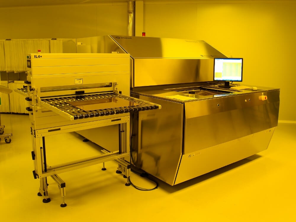
Laser Direct Imaging, often abbreviated as LDI, represents a significant advancement in the field of printed circuit board manufacturing. This technology utilizes precise laser beams to directly transfer circuit patterns onto PCB substrates, eliminating the need for traditional photomasks. By doing so, it enhances accuracy and reduces production errors. For electric engineers, understanding LDI is crucial as it directly impacts registration quality, production efficiency, and the ability to handle complex designs. This article explores how a system improves registration quality with linear and nonlinear transformations, incorporates UV diode lasers that achieve lifetimes, or mean time between failures (MTBF), of over 25,000 hours, and enables the capability to simultaneously image multiple smaller PCBs in a single run. The following sections provide a deep dive into the technical aspects and practical benefits of this innovative approach.
What Is Laser Direct Imaging and Why It Matters
Laser Direct Imaging is a modern photolithography technique used in PCB manufacturing to create highly accurate circuit patterns. Unlike conventional methods that rely on physical masks, LDI employs a computer-controlled laser to expose photosensitive layers on the PCB substrate. This results in finer line resolutions and improved alignment precision, which are essential for high-density interconnect boards. For electric engineers, the importance of LDI lies in its ability to support miniaturization trends and meet stringent industry standards. It reduces defects associated with mask misalignment and enables rapid prototyping by streamlining the imaging process. As PCB designs grow more intricate, adopting technologies that enhance precision and efficiency becomes indispensable for maintaining quality and performance in electronic products.
Technical Principles of Laser Direct Imaging
Laser Direct Imaging operates by directing a focused laser beam onto a photosensitive resist layer applied to the PCB substrate. The laser is guided by digital data from the circuit design, ensuring exact replication of patterns without physical intermediaries. A key aspect of LDI technology is its use of UV diode lasers, which provide the necessary wavelength for high-resolution imaging. These lasers are engineered for durability, often achieving lifetimes, expressed as MTBF, of over 25,000 hours. This longevity minimizes downtime and maintenance costs in high-volume production environments.
Another critical feature is the application of linear and nonlinear transformations to enhance registration quality. Linear transformations adjust for uniform scaling and rotation issues, ensuring consistent alignment across the panel. Nonlinear transformations address more complex distortions, such as those caused by material irregularities or thermal expansion. By applying these corrections, the system improves registration quality with linear and nonlinear transformations, achieving sub-micron accuracy. This precision is vital for multilayer boards where even minor misalignments can lead to functional failures.
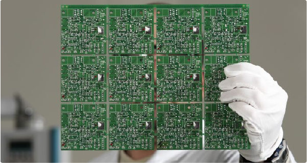
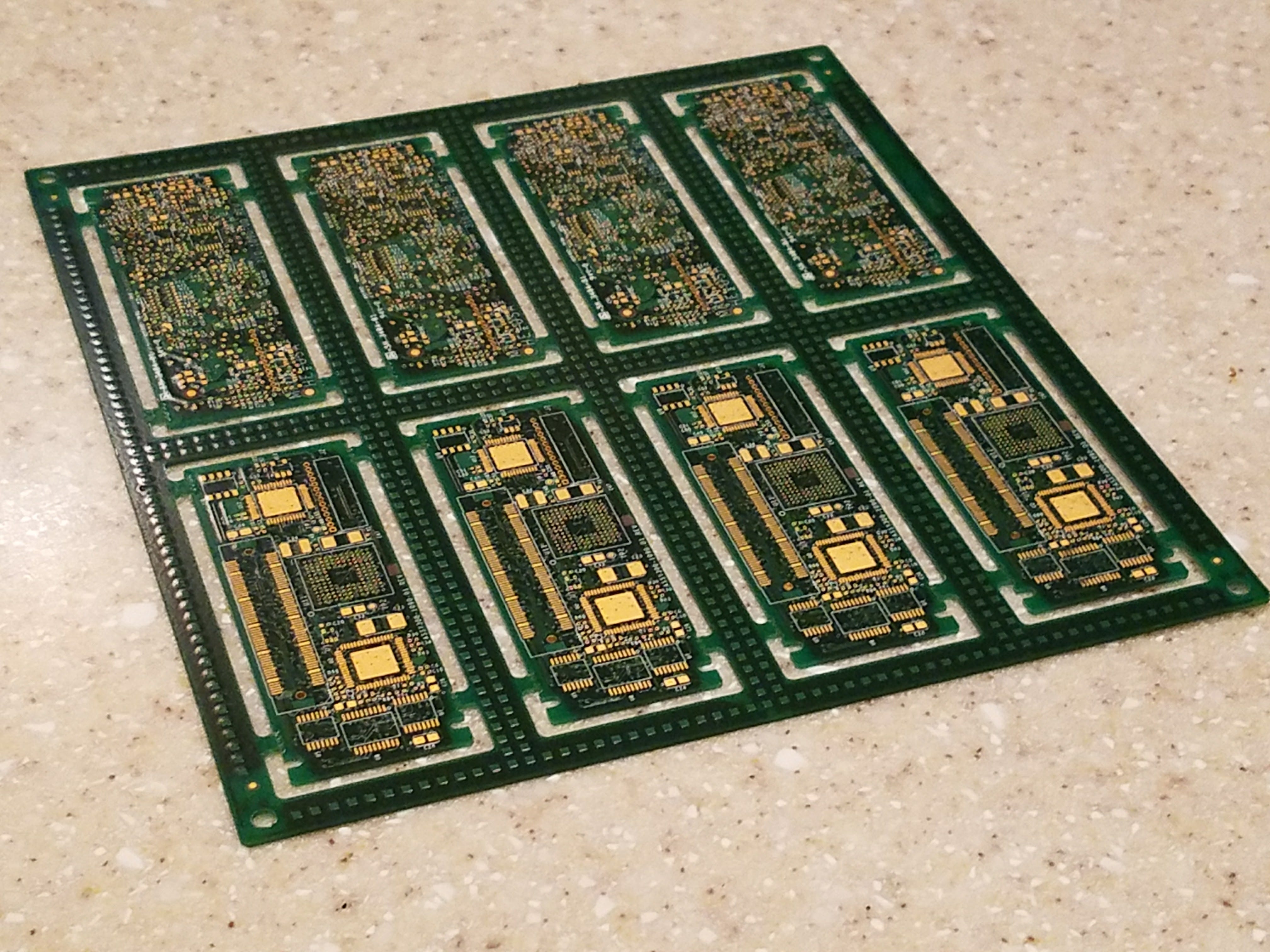
Additionally, advanced LDI systems can simultaneously image multiple smaller PCBs in a single run. This capability is enabled by sophisticated software algorithms that partition the imaging area into discrete sections, each corresponding to an individual board layout. Such parallel processing significantly boosts throughput, making it ideal for batch production of compact electronic devices.
Benefits of Laser Direct Imaging for PCB Manufacturing
The adoption of LDI technology brings several advantages to PCB manufacturing, particularly for electric engineers focused on quality and efficiency. First, the elimination of photomasks reduces production steps and associated costs. It also minimizes errors stemming from mask wear or misalignment, directly improving yield rates. The precision offered by UV diode lasers, with MTBF exceeding 25,000 hours, ensures consistent performance over extended periods, supporting uninterrupted manufacturing cycles.
Furthermore, the ability to simultaneously image multiple smaller PCBs in a single run optimizes resource use and accelerates delivery timelines. This feature is especially beneficial for prototypes or small-batch runs where diverse designs must be processed quickly. The system's capacity to apply linear and nonlinear transformations also ensures that registration quality remains uncompromised, even when imaging varied panel layouts. These benefits collectively enhance the reliability and scalability of PCB production, meeting the rigorous demands of modern electronics.
Practical Applications and Best Practices
Implementing Laser Direct Imaging in a manufacturing setup requires adherence to specific practices to maximize its potential. Electric engineers should ensure that the digital design files used for imaging are optimized for LDI systems. This involves verifying that the data accounts for material properties and potential distortions, enabling accurate application of linear and nonlinear transformations. Regular calibration of the laser system is also essential to maintain precision and uphold the registration quality across production runs.
When leveraging the capability to simultaneously image multiple smaller PCBs in a single run, engineers must carefully plan the panel layout. Efficient nesting of smaller boards within the imaging area reduces material waste and enhances throughput. It is advisable to group designs with similar exposure requirements to streamline the process. Additionally, selecting UV diode lasers with proven MTBF of over 25,000 hours ensures long-term reliability, minimizing interruptions due to equipment failure.
Monitoring environmental conditions, such as temperature and humidity, in the imaging facility is another critical practice. These factors can influence material behavior and, consequently, the effectiveness of registration corrections. Adhering to guidelines set by recognized industry standards, such as IPC-6012E, helps maintain consistent quality during LDI implementation.
Challenges and Solutions in Laser Direct Imaging
While LDI offers numerous advantages, certain challenges must be addressed to ensure optimal performance. One common issue is the initial setup complexity, as integrating digital imaging systems into existing workflows can require significant adjustments. Engineers can mitigate this by conducting thorough training sessions and developing standardized operating procedures aligned with industry benchmarks like IPC-A-600K.
Another challenge is the potential for laser degradation over time, despite the robust MTBF of over 25,000 hours for UV diode lasers. To counter this, implementing a proactive maintenance schedule based on usage patterns helps sustain laser performance. Additionally, when imaging multiple smaller PCBs in a single run, discrepancies in substrate flatness can affect registration. Applying advanced transformation algorithms, including both linear and nonlinear corrections, effectively compensates for such variations, ensuring uniform quality.
Data management also poses a challenge, given the high volume of design information processed during LDI operations. Utilizing secure, high-capacity storage solutions and maintaining version control prevents data loss or errors. By addressing these challenges with systematic solutions, engineers can fully harness the precision and efficiency of LDI technology.
Conclusion
Laser Direct Imaging stands as a transformative technology in PCB manufacturing, offering unparalleled accuracy and efficiency for electric engineers. By employing UV diode lasers with lifetimes, or MTBF, exceeding 25,000 hours, it ensures sustained performance in demanding production environments. The system's ability to improve registration quality with linear and nonlinear transformations addresses alignment challenges, while the capacity to simultaneously image multiple smaller PCBs in a single run enhances productivity. As the electronics industry continues to push boundaries with complex designs and miniaturization, adopting LDI becomes a strategic imperative. Through adherence to best practices and industry standards, manufacturers can achieve consistent quality and reliability, paving the way for innovation in electronic product development.
FAQs
Q1: How does a system improve registration quality with linear and nonlinear transformations in LDI?
A1: Linear transformations correct for uniform scaling and rotational misalignments during PCB imaging, ensuring consistent alignment. Nonlinear transformations tackle complex distortions from material inconsistencies or thermal effects. Together, they achieve sub-micron precision, vital for multilayer boards. This approach, integral to advanced LDI systems, significantly reduces errors as per standards like IPC-6012E.
Q2: What is the significance of UV diode lasers achieving MTBF of over 25,000 hours in PCB imaging?
A2: UV diode lasers with an MTBF exceeding 25,000 hours offer exceptional reliability in LDI processes. This longevity reduces downtime and maintenance frequency, ensuring continuous operation in high-volume PCB production. For electric engineers, it translates to cost efficiency and consistent imaging quality over extended periods.
Q3: How does LDI technology simultaneously image multiple smaller PCBs in a single run?
A3: LDI systems use sophisticated software to partition the imaging area into sections for different PCB layouts. This allows parallel processing of multiple smaller boards on one panel, boosting throughput. It’s ideal for prototyping or small-batch production, optimizing material use and reducing cycle times for engineers.
Q4: What standards guide the use of Laser Direct Imaging in PCB manufacturing?
A4: Standards like IPC-6012E for rigid board performance and IPC-A-600K for board acceptability provide guidelines for LDI implementation. These ensure imaging precision and quality control, helping engineers maintain consistency in registration and pattern accuracy during production processes.
References
IPC-6012E — Qualification and Performance Specification for Rigid Printed Boards. IPC, 2020.
IPC-A-600K — Acceptability of Printed Boards. IPC, 2020.


