Introduction
In modern PCB manufacturing, depaneling represents a critical final step where individual boards are separated from production panels. Traditional mechanical methods often introduce stress that can compromise board integrity, especially as designs trend toward higher densities and flexible substrates. Laser PCB depaneling emerges as a superior alternative, delivering precise cuts with negligible mechanical force. This approach minimizes issues like microcracking and delamination, aligning with the demands of electric engineers focused on reliability in high-performance applications. By leveraging non-contact ablation, laser processes ensure cleaner edges and reduced contamination. As miniaturization advances, understanding laser PCB depaneling becomes essential for optimizing yield and performance.
What Is Laser PCB Depaneling and Why It Matters
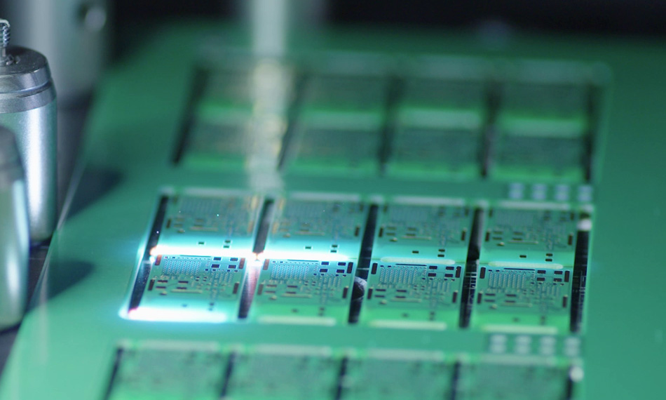
Laser PCB depaneling involves using a focused laser beam to ablate material along predefined contours, separating boards without physical contact. Unlike routing or shearing, this method vaporizes thin layers iteratively, producing kerf widths as fine as tens of microns. It matters profoundly in industries requiring high precision, such as aerospace and medical devices, where even minor stress can propagate failures during assembly or operation. For electric engineers, the relevance lies in maintaining signal integrity and mechanical stability post-depaneling. Production panels with dozens of boards benefit from this scalability, supporting high-mix, low-volume runs common in prototyping. Ultimately, it addresses the limitations of mechanical stress in achieving defect-free boards compliant with quality benchmarks.
Technical Principles of Laser PCB Cutting
The core mechanism of laser PCB cutting relies on photothermal or photochemical ablation, depending on laser parameters. UV lasers, typically at 355 nm wavelength, excel in breaking molecular bonds in epoxy resins like FR4, enabling cold ablation with minimal heat-affected zones. Pulse durations range from nanoseconds to femtoseconds, where shorter pulses reduce thermal diffusion and collateral damage. Fluence, or energy per unit area, must be tuned above the ablation threshold yet below plasma formation to avoid recast layers. Repetition rates and scan speeds control throughput, while galvo scanners ensure sub-micron positional accuracy. These principles collectively minimize PCB depaneling stress by eliminating vibration and force application inherent in mechanical tools.
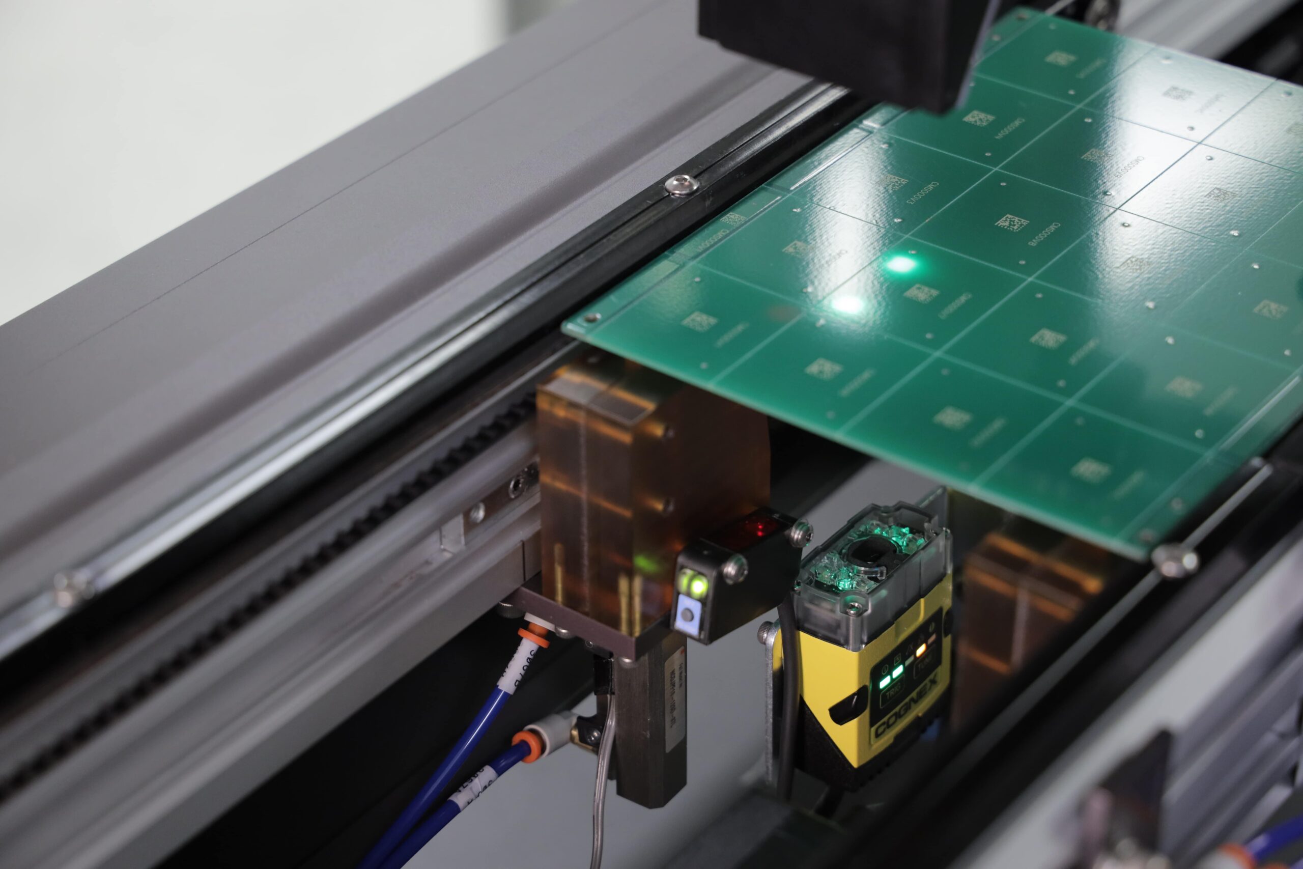
In practice, the process starts with fiducial alignment via machine vision, followed by vector or raster scanning paths. For rigid boards, multiple passes may layer-remove copper and dielectric. Flex PCBs demand adjusted parameters to handle polyimide without charring. Beam shaping optics further refine spot size, optimizing for contour complexity. Electric engineers appreciate how these controllable variables predict outcomes, facilitating simulation-driven optimization. This precision underpins compliance with edge quality requirements in manufacturing standards.
How Laser Depaneling Minimizes Stress Compared to Mechanical Methods
Mechanical routing employs high-speed spindles with diamond bits, generating forces that induce tensile stress and potential microcracks in vias or traces. Laser depaneling, by contrast, applies no lateral force, preserving laminate flatness and preventing warpage. Post-process measurements using IPC-TM-650 2.4.22 reveal significantly lower bow and twist in laser-depaneled boards versus routed ones. Stress concentrations at corners, common in punching, are eliminated through smooth, tapered laser kerfs. Dust and burrs from routing contaminate cleanrooms, whereas laser ablation produces gaseous byproducts easily extracted. For engineers, this translates to higher assembly yields, as reduced stress mitigates tombstoning or floating components during reflow.
Quantitative stress analysis via strain gauges, guided by IPC/JEDEC-9704, confirms lasers maintain strains below critical thresholds. Thermal effects, though present, are localized and transient, unlike sustained heating in sawing. This non-contact nature suits thin boards prone to snapping. Engineers can model stress fields using FEA, validating laser paths pre-production. Overall, the shift to laser reduces field failures linked to latent depaneling damage.
Laser Depaneling vs Routing: A Detailed Comparison
Routing dominates high-volume rigid board production due to speed but falters on intricate tabs or flex circuits. Laser depaneling handles arbitrary geometries without tooling changes, ideal for rapid prototyping. Tool wear in routers necessitates frequent replacements, increasing downtime, while lasers offer consistent performance over millions of cuts. Edge roughness from routing averages higher, risking solder mask delamination, whereas laser edges exhibit Ra values suitable for fine-pitch assembly. Throughput comparisons favor routing for simple panels, but lasers excel in complexity. Cost-wise, laser depaneling equipment demands higher upfront investment, offset by no consumables and lower scrap rates.
Stress metrics highlight the divergence: routing vibrates panels, amplifying bow beyond IPC-6012 allowances for surface-mount boards. Lasers avoid this, supporting tighter tolerances. Fixturing for routing risks board deflection, absent in vacuum-held laser systems. For HDI boards with microvias, laser precision prevents via barrel damage. Engineers weigh these factors based on panel yield and design rules.
- Stress Introduction — Laser: Minimal (non-contact); Mechanical: High (vibration, force)
- Edge Quality — Laser: Smooth, tapered kerf; Mechanical: Burrs, potential chipping
- Tooling — Laser: None required; Mechanical: Bits wear out
- Flexibility — Laser: Any contour, no setup; Mechanical: Limited by bit diameter
- Byproducts — Laser: Gaseous, extractable; Mechanical: Dust, requires suppression
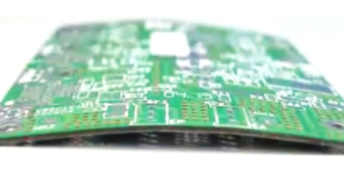
Laser Depaneling for Flex PCBs: Specialized Considerations
Flex and rigid-flex PCBs pose unique challenges due to their thin, pliable substrates. Laser depaneling shines here, as mechanical tension easily tears copper foils or creases dielectrics. UV laser depaneling penetrates polyimide cleanly, preserving flexibility without hardening. Parameters shift to lower fluence for polymers, avoiding melting. Scoring techniques enable partial cuts for manual separation, reducing full ablation time. Electric engineers value this for wearables and automotive sensors, where bend radius integrity is paramount.
Assist gases like nitrogen aid in clearing debris without oxidation. Vision systems compensate for substrate curl during processing. Post-depaneling flex tests confirm no stiffness increase. This method supports high-density interconnects on flex without delamination risks.
Key Factors in Laser Depaneling Equipment Selection
Selecting laser depaneling equipment involves balancing laser source, optics, and automation. UV diode-pumped solid-state lasers provide reliability for FR4, while fiber lasers suit metals. Dual-beam systems accelerate processing. Software integrates Gerber data for fiducial teaching and path optimization. Throughput depends on panel size and board count, with indexers for continuous flow. Maintenance focuses on optics cleaning and calibration.
Cost components include capital for the system, operational for power and gases, and scaling with utilization. Engineers prioritize uptime metrics and integration with MES. Yield tracking post-installation validates ROI through defect reduction.
Best Practices for Laser PCB Depaneling Implementation
Begin with design-for-depaneling: incorporate fiducials, avoid acute angles exceeding beam divergence. Parameter development uses DOE to dial fluence, speed, and passes for material stacks. In-line metrology verifies kerf width and HAZ via microscopy. Vacuum extraction prevents re-deposition. Factory protocols align with IPC-A-600 for edge acceptability, inspecting for char or taper.
Operator training emphasizes safety interlocks and alignment. Process control charts monitor warpage per IPC-TM-650 2.4.22. For flex, humidity control mitigates static. Scaling involves parallel stations for volume. Engineers iterate via SPC, ensuring consistency.
Challenges in Laser Depaneling and Mitigation Strategies
One challenge is heat-affected zone in thicker stacks, mitigated by ultrafast pulses fragmenting material cold. Recast on copper demands higher energy or chemistry aids. Tapering from beam geometry requires bidirectional scanning. Throughput lags mechanical for bulk, addressed by multi-axis motion. Residue inspection uses UV fluorescence.
For high Tg laminates, pre-heating stabilizes ablation. Engineers employ DOE and modeling to preempt issues. Validation against IPC-6012 ensures performance.
Conclusion
Laser PCB depaneling achieves unparalleled precision and minimal stress, revolutionizing separation for rigid, flex, and advanced boards. By ablating without force, it preserves integrity, reduces warpage, and enhances yields. Comparisons underscore superiority over routing in quality-critical apps. Best practices and equipment savvy maximize benefits. Electric engineers gain reliable processes aligning with standards like IPC-TM-650 2.4.22. Adopting this technology future-proofs manufacturing against miniaturization demands.
FAQs
Q1: What is laser PCB depaneling?
A1: Laser PCB depaneling uses a focused beam to ablate panel material along board outlines, separating units non-contact. UV wavelengths target organics precisely, minimizing damage. It suits complex shapes and flex substrates. Factory insights emphasize its role in stress-free production per quality specs.
Q2: How does laser PCB depaneling reduce PCB depaneling stress?
A3: It eliminates mechanical forces, preventing microcracks and warpage seen in routing. Measurements per IPC-TM-650 2.4.22 show lower bow values. Thermal effects stay localized via short pulses. Engineers benefit from reliable boards for assembly.
Q3: What are the advantages of laser depaneling vs routing?
A3: Laser offers tool-free flexibility, cleaner edges, and no vibration stress. Routing suits volume but generates dust and wear. Laser excels for prototypes and HDI. Cost balances via reduced scrap.
Q4: Is laser depaneling suitable for flex PCBs?
A4: Yes, UV laser depaneling cuts polyimide cleanly without tearing foils. Adjusted parameters preserve bendability. It handles scoring for partial separation. Ideal for dynamic applications.
References
IPC-TM-650 2.4.22C — Test Methods Manual, Bow and Twist. IPC, 2022
IPC-6012E — Qualification and Performance Specification for Rigid Printed Boards. IPC, 2015
IPC/JEDEC-9704 — Strain Gage Characterization for PCB Assembly Process Control. IPC/JEDEC, 2012


