Introduction
For electronic hobbyists eager to prototype circuits without waiting for factory orders, laser PCB etching at home offers an accessible entry into custom board creation. This method combines modern laser technology with traditional chemical etching to produce functional printed circuit boards right in your workspace. Unlike older techniques that rely on printers and ironing, a laser PCB etching machine streamlines the process by precisely removing a protective mask from copper-clad boards. Hobbyists appreciate the control and repeatability it provides for single or double-sided designs. In this guide, we cover everything from setup to finishing, ensuring you achieve reliable results safely and efficiently. Whether you're building simple LED drivers or microcontroller projects, etching home with a laser opens up endless experimentation.
What Is Laser PCB Etching and Why It Matters for Hobbyists
Laser PCB etching involves using a laser PCB machine to ablate a temporary mask on a copper-clad board, exposing areas for chemical removal of unwanted copper. The laser does not directly vaporize the copper foil in most home setups; instead, it clears paint or a similar coating, allowing etchant to dissolve the metal precisely. This hybrid approach suits beginners because it leverages affordable diode lasers common in hobby engravers. For electronic hobbyists, it matters due to rapid iteration—design, etch, test, and revise in hours rather than days. Traditional methods like toner transfer often suffer from alignment issues or blurry traces, while laser precision minimizes those flaws. Ultimately, this technique empowers makers to tackle surface-mount components and compact layouts at home.
Technical Principles Behind Laser PCB Etching
The core principle relies on selective ablation, where the laser's focused beam vaporizes the mask material without significantly affecting the underlying copper. Diode lasers, typically in the blue-violet spectrum, excel at this because organic paints absorb their wavelength efficiently, leading to clean removal after multiple passes. Copper reflects much of the laser energy, preventing direct etching unless using specialized high-power fiber lasers, which are less common for starters. After mask removal, chemical etchants like ferric chloride or persulfate solutions react with exposed copper, undercutting slightly to define traces. Proper focus and speed control trace width and edge quality, mimicking professional subtractive manufacturing. Understanding these interactions helps hobbyists optimize settings for consistent outcomes.
Heat from the laser can cause minor residue buildup if airflow is inadequate, so multiple passes ensure complete exposure. The board substrate, usually FR4 fiberglass, remains inert throughout, providing mechanical stability. This method aligns with factory-driven insights on pattern definition, where mask integrity directly impacts final conductor geometry.
Essential Equipment and Materials for Etching Home
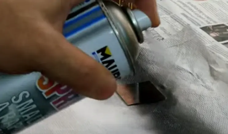
To start etching home, assemble a basic laser PCB etching machine setup with a diode laser engraver capable of handling small boards. Key materials include double-sided copper-clad FR4 blanks, matte black spray paint as the etch mask, and a chemical etchant such as ferric chloride or sodium persulfate. Software like open-source engravers converts PCB designs into raster images for laser control, using threshold modes for sharp edges. Additional tools cover isopropyl alcohol for cleanup, sponges for etching agitation, painters tape for alignment, and a plastic tray for the etch bath. Ventilation is crucial, along with laser safety glasses matched to your machine's wavelength. This kit keeps costs low while enabling professional-looking prototypes.
Safety Considerations for Laser PCB Machine Use
Safety forms the foundation of any home etching project, starting with laser hazards classified under IEC 60825-1 standards. Diode engravers often fall into higher classes requiring enclosed operation or protective eyewear to prevent eye damage from stray reflections. Fumes from ablating paint demand strong exhaust or outdoor use to avoid respiratory issues. Chemical etchants are corrosive, so gloves, aprons, and eyewear protect skin, with neutralization for waste disposal. Fire risk exists from flammable paints or etchant vapors near heat sources, so keep extinguishers handy. Following these practices ensures hobbyists can focus on creativity without risks.
Step-by-Step Guide to Laser PCB Etching at Home
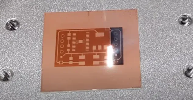
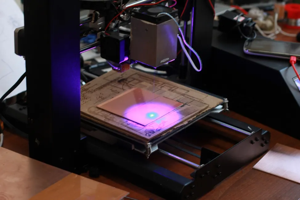
Begin by preparing your PCB design in software, exporting as a high-resolution black-and-white image where black represents areas to etch. Cut the copper-clad board to size, lightly sand for adhesion, clean with alcohol, and apply two thin coats of matte black spray paint, drying fully between layers. Secure the board in the laser PCB etching machine, load the inverted image (white traces on black), and set parameters like moderate power with slow speed for initial tests. Run multiple passes to fully remove paint from trace paths, flipping for double-sided boards and aligning via fiducials or tape. Submerge or dab etchant onto exposed copper, agitating gently until clear, typically monitoring for 10-30 minutes depending on concentration. Rinse thoroughly, strip remaining paint with alcohol, and inspect for continuity.
For double-sided etching, engrave one side, flip precisely using reference holes, and repeat before etching to maintain registration.
Best Practices and Troubleshooting for Optimal Results
Achieve finer traces by experimenting with laser speed and passes—slower with higher power cleans residue better, while defocusing slightly narrows lines. Ensure even paint thickness to prevent under- or over-etching, and use cardboard shims for perfect focus. Agitate etchant uniformly to avoid uneven dissolution, and stop promptly to minimize undercutting. Common issues like misalignment stem from loose boards; tape securely or add jigs. Residue after laser work? Increase passes or improve airflow. For quality, check traces against IPC-A-600 acceptability criteria, such as uniform conductor width and no bridging.
Post-etch, optional steps include drilling holes with a press and applying solder mask via similar paint-and-laser methods for protection.
Inspecting and Ensuring PCB Quality
Home-etched boards should meet basic IPC-6012 performance specs for rigid boards, focusing on conductor integrity and spacing. Visually inspect for pinholes, excessive underetch, or mouse bites per IPC-A-600 guidelines, rejecting boards with defects that could cause shorts or opens. Continuity testing with a multimeter confirms functionality before soldering. Proper etching preserves copper thickness for current handling, vital for hobby projects. Document your process to refine future runs, aligning home efforts with industry benchmarks.
Advantages of Laser PCB Etching Over Traditional Methods
This approach outshines toner transfer by eliminating printer limitations and transfer failures, offering sharper definition via digital control. Chemical etching alone requires precise masking, but lasers handle complex geometries effortlessly. Hobbyists gain flexibility for revisions without reprinting films. Compared to outsourcing, it's cost-effective for low volumes, fostering skill-building. While not for high-volume production, it bridges prototyping gaps perfectly.
Conclusion
Laser PCB etching at home transforms hobbyists into self-sufficient makers, delivering precise prototypes with minimal gear. By mastering mask ablation and chemical processing, you unlock fast iteration for innovative circuits. Adhere to safety like IEC 60825-1 and quality standards for dependable boards. Experiment confidently, starting simple and scaling to soldermask or multi-layer. This guide equips you to embrace etching home fully.
FAQs
Q1: What is a laser PCB etching machine, and is it suitable for beginners etching home?
A1: A laser PCB etching machine is typically a diode engraver that removes paint masks from copper boards for subsequent chemical etching. Beginners find it approachable due to simple software and affordable models, requiring only basic settings like power and speed. It outperforms manual methods in precision, enabling fine traces for hobby projects. Always prioritize safety gear for smooth starts.
Q2: How does a laser PCB machine improve etching home compared to photoresist?
A2: Laser PCB machines simplify patterning by directly ablating masks without UV exposure or film alignment hassles common in photoresist. Multiple passes ensure clean exposure, speeding up the workflow for hobbyists. Results show better registration for double-sided boards. Combined with agitation during etching, it yields reliable traces meeting basic quality needs.
Q3: What safety standards apply when using a laser PCB etching machine at home?
A3: IEC 60825-1 classifies lasers and mandates eyewear plus enclosures for engravers. Ventilation handles paint fumes, while gloves protect against etchants. These prevent eye, skin, or inhalation risks during etching home. Proper setup keeps operations safe for ongoing hobby use.
Q4: Can laser PCB etching produce boards compliant with industry quality like IPC standards?
A4: Yes, home laser etching can achieve IPC-A-600 acceptable features, such as smooth conductors without bridging, through careful mask removal and etching control. Inspect for uniformity post-process. It suits prototypes where hobbyists verify functionality before assembly.
References
IPC-A-600K — Acceptability of Printed Boards. IPC, 2020
IPC-6012E — Qualification and Performance Specification for Rigid Printed Boards. IPC, 2017
IEC 60825-1:2014 — Safety of laser products – Part 1: Equipment classification and requirements. IEC, 2014