Introduction
For electronic hobbyists starting their journey into printed circuit board design, CEM-1 offers an accessible entry point. This material enables the creation of simple, cost-effective single-sided boards perfect for prototyping basic circuits like LED drivers or sensor interfaces. Unlike more advanced substrates, CEM-1 prioritizes affordability without sacrificing basic functionality for low-power applications. Mastering CEM-1 PCB design rules lays a strong foundation for understanding PCB design for hobbyists. This guide walks beginners through essential concepts, from material basics to layout strategies and prototyping tips. By following structured approaches, hobbyists can produce reliable boards that perform well in personal projects.
What Is CEM-1 and Why Does It Matter for Hobbyists?
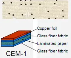
CEM-1, or Composite Epoxy Material grade 1, consists of a cellulose paper core reinforced with woven glass cloth and epoxy resin, making it suitable primarily for single-sided PCBs. This composition results in a lightweight, economical substrate that hobbyists appreciate for quick prototypes and low-volume builds. Compared to higher-grade materials like FR-4, CEM-1 provides adequate electrical insulation and mechanical support for straightforward designs but has limitations in thermal and flexural strength. Its relevance stems from widespread use in consumer electronics and educational kits, where complex multilayer routing is unnecessary. Hobbyists benefit from CEM-1's ease of processing, which aligns with home fabrication methods. Understanding these traits ensures designs stay within the material's capabilities, avoiding common pitfalls like delamination under stress.
Key Properties and Limitations of CEM-1
CEM-1 exhibits good flame retardancy and solderability, key for hand-assembly in hobbyist workshops. The paper-based core absorbs less moisture than pure phenolics, improving stability during storage. However, it demands careful handling to prevent warpage from uneven heating or mechanical loads. Electrical properties support low-frequency signals effectively, suiting audio amplifiers or simple controllers. Mechanical characteristics favor thin boards, reducing weight for battery-powered gadgets. Always consult IPC-4101 for base material specifications to match project needs accurately.
While cost savings drive its popularity, CEM-1 falls short in high-temperature environments or applications requiring vias, as the core resists through-plating. Hobbyists should reserve it for single-layer layouts to leverage its strengths fully. Pairing it with appropriate copper weights enhances current handling without excess thickness.
Essential CEM-1 PCB Design Rules
Adhering to CEM-1 PCB design rules prevents manufacturing defects and ensures board reliability. Start with conservative trace widths and spacings to account for the material's etching sensitivity. Annular rings around pads must provide sufficient copper overlap for robust soldering. Avoid sharp corners in traces to minimize stress concentrations that could lead to cracks. Hole sizes should align with standard drill bits available for prototyping services. Compliance with IPC-2221 guidelines for generic PCB design reinforces these practices across layers and materials.
Pad shapes influence solder joint integrity, so opt for round or oval geometries on single-sided boards. Clearance between components prevents shorting during manual assembly. Ground connections benefit from dedicated pours where possible, reducing noise in analog sections. These rules form the backbone of successful CEM-1 PCB prototyping.
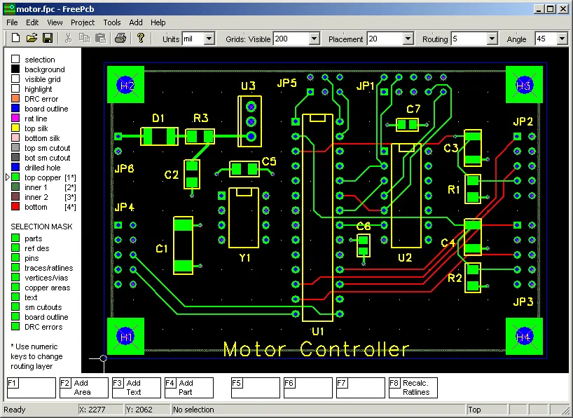
Single-Sided PCB Layout Tutorial: Step-by-Step for Beginners
Begin PCB design for hobbyists by sketching a schematic to map connections logically. Place components starting with high-power elements like resistors or ICs farthest from edges to aid heat dissipation. Group related functions, such as power inputs near regulators, to shorten traces and minimize loops. Route signals on the copper side without crossings, using jumpers only if essential for complex nets.
Next, optimize trace paths for even copper distribution, preventing warpage in CEM-1 boards. Add silkscreen labels for easy identification during assembly. Verify netlist integrity to catch errors early. Generate Gerber files with outline layers for precise fabrication.
Finalize by running design rule checks for spacing violations. This single-sided PCB layout tutorial emphasizes simplicity, ideal for CEM-1's constraints. Test virtually with simulators before committing to prototypes.
Choosing and Using CEM-1 PCB Design Software
Selecting the right CEM-1 PCB design software simplifies the learning curve for beginners. Look for intuitive interfaces with drag-and-drop placement and auto-routing features tailored to single-layer boards. Free options abound for hobbyists, offering schematic capture integrated with layout editors. These tools enforce basic design rules, flagging issues like inadequate clearances proactively.
Import footprints from standard libraries matching through-hole components common in CEM-1 projects. Customize grid settings for precise alignment on paper-based substrates. Export formats must include drill files for prototyping compatibility. Practice with sample projects to build confidence in handling CEM-1 specifics.
Software with 3D previews helps visualize assembly challenges early. Hobbyists gain efficiency by mastering layers management despite single-sided limitations. This approach turns complex ideas into fabricable designs swiftly.
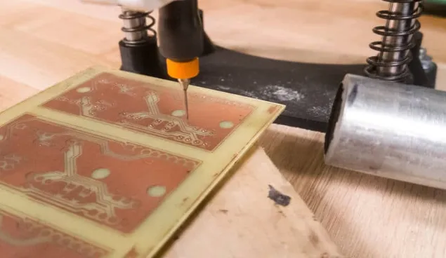
Best Practices for CEM-1 PCB Prototyping
Prototyping CEM-1 boards starts with panelizing designs for cost efficiency in small runs. Specify copper thickness suited to current demands, typically standard foils for hobby use. Etching processes tolerate CEM-1 well, but mask application requires uniformity to avoid undercuts. Post-etch cleaning removes residues that could impair solderability.
For quality assurance, inspect for warpage visually and mechanically. Solder components using low-heat irons to preserve material integrity, following IPC-A-600 criteria for acceptability. Bake boards pre-assembly if stored in humid conditions. These steps ensure prototypes match production intent.
Incorporate test points for debugging without compromising layout density. Iterate based on electrical testing to refine future designs. CEM-1 PCB prototyping thrives on methodical validation.
Troubleshooting Common CEM-1 Design Issues
Hobbyists often encounter trace lifts due to aggressive soldering; mitigate by using flux sparingly and pre-tinning pads. Warpage arises from asymmetric copper; balance pours across the board. Poor adhesion in humid environments calls for desiccated storage. Signal noise in unshielded layouts improves with bypass capacitors near ICs.
Delamination risks increase with overbaking; limit exposure times. Component misalignment stems from loose fixtures during assembly. Addressing these systematically enhances reliability.
Conclusion
Mastering CEM-1 PCB design equips hobbyists with practical skills for affordable prototyping. From understanding material limits to applying single-sided layout principles, each step builds competence. Key takeaways include conservative rules, software proficiency, and thorough testing. These practices align with industry standards, fostering reliable outcomes. Experiment confidently, iterating toward polished projects. CEM-1 remains a staple for creative electronics exploration.
FAQs
Q1: What are the main CEM-1 PCB design rules for beginners?
A1: CEM-1 PCB design rules emphasize wider traces and spacings than advanced materials to suit its properties. Prioritize annular ring integrity and avoid vias for single-sided layouts. Balance copper distribution to prevent warpage. Follow IPC-2221 for general guidelines on clearances and pad geometries. This ensures etchability and solder joint strength in hobbyist prototypes.
Q2: How does a single-sided PCB layout tutorial help with CEM-1 projects?
A2: A single-sided PCB layout tutorial guides component grouping, trace routing without crossings, and silkscreen addition for clarity. It stresses power placement and ground optimization on CEM-1. Beginners learn to generate Gerbers efficiently. This structured process minimizes errors in PCB design for hobbyists, yielding functional boards quickly.
Q3: What should hobbyists consider in CEM-1 PCB design software?
A3: CEM-1 PCB design software should feature easy schematic-to-layout flow and rule checks for single-layer constraints. Seek free tools with footprint libraries for through-hole parts. 3D views aid assembly planning. These enable precise prototyping without steep learning curves, ideal for PCB design for hobbyists.
Q4: Why is CEM-1 popular for PCB prototyping among beginners?
A4: CEM-1 suits CEM-1 PCB prototyping due to low cost and simple processing for single-sided boards. It handles basic circuits reliably without high-end equipment. Etching and hand-soldering align with home setups. Limitations encourage good design habits early. Hobbyists achieve quick results for testing ideas effectively.
References
IPC-4101 — Specification for Base Materials for Rigid and Multilayer Printed Boards. IPC.
IPC-2221A — Generic Standard on Printed Board Design. IPC.
IPC-A-600K — Acceptability of Printed Boards. IPC.