Introduction
Printed Circuit Board (PCB) prototype design stands as a critical phase in the development of electronic products. For electrical engineers, creating a functional and reliable prototype is the foundation for testing concepts, validating performance, and ensuring manufacturability. A well designed prototype can save time, reduce costs, and prevent costly errors during full scale production. This article dives into PCB design tips and PCB prototype best practices to help engineers avoid common pitfalls. It also covers strategies for improving PCB performance and adhering to PCB layout guidelines. By focusing on proven methods and industry standards, this guide aims to equip professionals with the knowledge needed to achieve success in their prototyping efforts. Let’s explore the key principles and practical steps to master this process.
What Is PCB Prototype Design and Why It Matters
PCB prototype design refers to the initial creation of a circuit board used to test and validate a concept before PCB mass production. This stage allows engineers to evaluate functionality, identify design flaws, and ensure compatibility with intended applications. Prototyping is not just a preliminary step; it serves as a bridge between theoretical design and real world performance. A poorly executed prototype can lead to delays, increased costs, and even product failure. For electrical engineers, understanding PCB prototype best practices is vital to meet project timelines and quality expectations. The process also ensures compliance with industry standards, which govern reliability and safety. By prioritizing precision in this phase, engineers can minimize risks and build confidence in their designs for subsequent production stages.
Technical Principles of Effective PCB Prototype Design
At the core of PCB prototype design lies a set of technical principles that dictate functionality and reliability. First, engineers must focus on schematic accuracy. A schematic acts as the blueprint, defining how components connect and interact. Errors at this stage can cascade into layout issues, so thorough validation is necessary. Another key principle is signal integrity, which ensures that electrical signals travel without distortion or interference. This requires careful consideration of trace impedance, crosstalk, and electromagnetic interference during the design process.
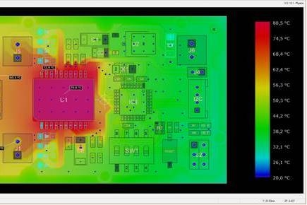
Thermal management is equally important. Components generate heat, and inadequate dissipation can degrade performance or cause failure. Engineers must account for heat dissipation paths and component placement to avoid hotspots. Power distribution also demands attention, as uneven voltage delivery can impact circuit behavior. Adhering to industry standards like IPC-2221B, which provides guidelines for design parameters, helps maintain consistency in these areas. These principles form the backbone of a prototype that performs as intended under real conditions.

PCB Prototype Best Practices for Electrical Engineers
To achieve a successful prototype, electrical engineers must follow established PCB design tips and best practices. Below are actionable strategies to guide the process.
Define Clear Design Specifications
Start by outlining the requirements of the prototype. This includes voltage levels, current ratings, environmental conditions, and intended applications. Clear specifications prevent scope creep and ensure that the design aligns with project goals. Refer to standards like IPC-6012E for performance and qualification criteria to set a reliable foundation.
Optimize Component Placement
Component placement directly impacts signal integrity and thermal performance. Place high speed components close to their connectors to minimize trace lengths. Group related components together to reduce interference. Also, ensure that heat generating parts are spaced to allow adequate cooling. Following PCB layout guidelines from standards such as IPC-2222A for sectional design can aid in achieving optimal placement.
Prioritize Trace Routing
Effective routing is essential for improving PCB performance. Keep traces as short and direct as possible to reduce signal delay. Avoid sharp angles in traces, as they can cause signal reflection. Separate high speed and analog signals from noisy power lines to prevent crosstalk. Adhering to IPC-2221B for trace width and spacing ensures electrical reliability.
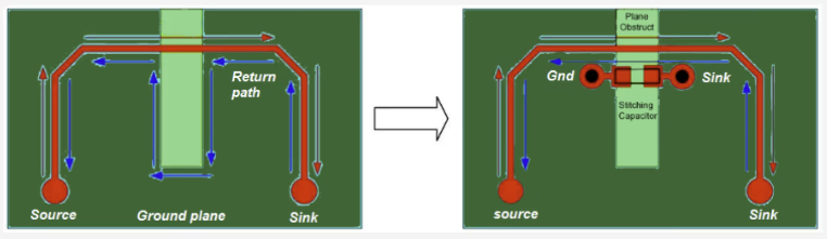
Incorporate Ground Planes
A solid ground plane reduces electromagnetic interference and provides a stable reference for signals. Use dedicated ground layers in multilayer boards to shield sensitive traces. If space allows, fill unused areas with ground copper to enhance shielding. This practice aligns with recommendations in industry standards for noise reduction.
Test and Iterate Early
Prototyping is an iterative process. Build and test the initial design to identify issues like signal loss or thermal stress. Use simulation tools to predict performance before fabrication. Early testing helps in avoiding PCB design mistakes that could persist into later stages. Standards like IPC-A-600K for board acceptability can guide inspection during testing.
Common Mistakes in PCB Prototype Design and How to Avoid Them
Even experienced engineers can encounter pitfalls during PCB prototype board design. Recognizing and avoiding PCB design mistakes is crucial for success. One frequent error is neglecting design for manufacturability. Failing to account for fabrication constraints, such as minimum trace widths or drill sizes, can lead to production issues. Consult standards like IPC-6012E to ensure designs meet manufacturing tolerances.
Another common issue is poor power distribution. Inadequate decoupling capacitors or uneven power traces can cause voltage drops, affecting performance. Place capacitors near power pins and use wide traces for power lines to mitigate this. Overlooking thermal management is also a recurring problem. Without proper heat dissipation, components may fail prematurely. Position heat sinks strategically and verify thermal paths during simulation.
Lastly, insufficient documentation often creates confusion during testing or production. Incomplete schematics or unclear labeling can delay troubleshooting. Maintain detailed records and follow PCB layout guidelines to ensure clarity. By addressing these errors proactively, engineers can save time and resources.
Strategies for Improving PCB Performance in Prototypes
Improving PCB performance starts with meticulous design choices. Focus on minimizing signal loss by using controlled impedance traces for high speed signals. This ensures consistent signal quality across the board. Additionally, select materials with appropriate dielectric constants to support signal integrity, guided by standards like JEDEC J-STD-020E for component and material compatibility.
Enhance power integrity by designing robust power distribution networks. Use multiple vias for high current paths to reduce resistance. Incorporate bypass capacitors at critical points to filter noise. Thermal performance can be improved by integrating thermal vias under hot components to transfer heat to other layers. Ensure that the stackup design supports both electrical and thermal needs, referencing IPC-2222A for multilayer configurations.
Finally, simulate the design under various conditions to predict performance. Simulation can reveal potential issues with signal timing or power delivery before physical prototyping. These strategies collectively contribute to a high performing PCB prototype.
Troubleshooting Insights for PCB Prototypes
Troubleshooting is an inevitable part of PCB prototype design. When issues arise, a systematic approach can pinpoint root causes efficiently. Begin by verifying the schematic against the physical board. Discrepancies in component values or connections often lead to unexpected behavior. Use standards like IPC-A-600K to inspect for visual defects such as solder bridging or misaligned traces.
If signal issues are suspected, check for noise or crosstalk using an oscilloscope. Long traces or poor grounding may be the culprit. Adjust routing or add shielding as needed. For thermal problems, measure component temperatures to identify overheating. Reposition components or enhance cooling if necessary. Document every test and modification to build a knowledge base for future designs. This methodical process ensures that issues are resolved without introducing new errors.
Conclusion
Mastering PCB prototype design requires a blend of technical expertise, adherence to industry standards, and attention to detail. By following PCB design tips and PCB prototype best practices, electrical engineers can create reliable and high performing prototypes. Avoiding PCB design mistakes through careful planning and testing saves time and resources. Strategies for improving PCB performance, such as optimizing signal integrity and thermal management, elevate the quality of the design. Additionally, structured troubleshooting ensures that issues are addressed effectively. With these insights and adherence to PCB layout guidelines, engineers can confidently navigate the complexities of prototyping and lay a strong foundation for successful production.
FAQs
Q1: What are the most critical PCB design tips for beginners?
A1: For beginners, focusing on schematic accuracy is vital among PCB design tips. Start with clear specifications and validate connections before layout. Keep traces short and avoid crossing high speed signals with power lines. Use ground planes to reduce noise. Always refer to industry standards like IPC-2221B for trace spacing and width. Early simulation and testing help catch errors before fabrication, ensuring a smoother prototyping process.
Q2: How can I avoid common PCB design mistakes in prototypes?
A2: Avoiding PCB design mistakes requires attention to manufacturability and thorough documentation. Ensure your design respects fabrication limits by consulting standards like IPC-6012E. Place decoupling capacitors near power pins to prevent voltage issues. Address thermal concerns by spacing heat generating components. Maintain detailed schematics and labels for clarity during testing. These steps minimize errors and streamline the debugging phase.
Q3: What are effective ways for improving PCB performance in early designs?
A3: Improving PCB performance starts with controlled impedance traces for signal integrity. Use robust power distribution with multiple vias and bypass capacitors to reduce noise. Enhance thermal management by adding thermal vias under hot components. Simulate designs to predict issues before building. Follow standards like IPC-2222A for stackup design to balance electrical and thermal needs. These practices ensure reliable prototype performance.
Q4: Why are PCB layout guidelines important for prototype success?
A4: PCB layout guidelines are crucial for ensuring functionality and manufacturability in prototypes. They dictate optimal component placement, trace routing, and grounding to minimize interference and signal loss. Standards like IPC-2221B provide rules for spacing and width, preventing electrical issues. Adhering to these guidelines reduces the risk of design flaws, supports efficient testing, and prepares the prototype for smooth transition to production.
References
IPC-2221B — Generic Standard on Printed Board Design. IPC, 2012.
IPC-2222A — Sectional Design Standard for Rigid Organic Printed Boards. IPC, 2010.
IPC-6012E — Qualification and Performance Specification for Rigid Printed Boards. IPC, 2020.
IPC-A-600K — Acceptability of Printed Boards. IPC, 2020.
JEDEC J-STD-020E — Moisture/Reflow Sensitivity Classification for Nonhermetic Surface Mount Devices. JEDEC, 2014.


