What is PCB X-ray Inspection and Why is it Essential for Quality?
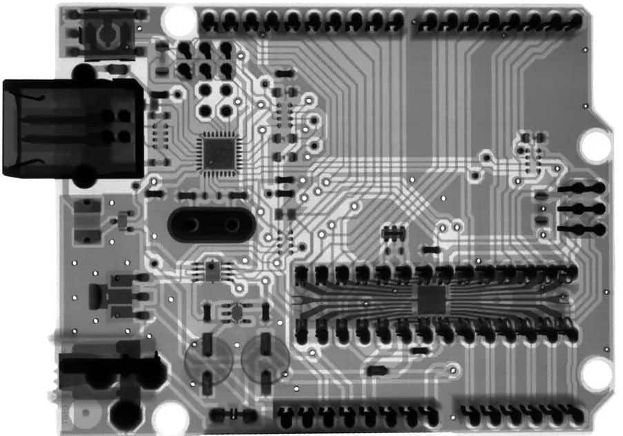
PCB X-ray inspection is a sophisticated, non-destructive method used to thoroughly examine the internal architecture of a printed circuit board. Unlike conventional visual inspections or automated optical inspection (AOI) techniques, which primarily focus on surface-level assessment, X-ray technology penetrates the board's layers. This allows it to reveal hidden flaws such as solder voids, misaligned components, or fractured connections that are otherwise invisible. This capability is particularly vital for contemporary PCBs with intricate designs, including those featuring Ball Grid Arrays (BGAs) or multi-layer constructions, where defects can be concealed beneath components or embedded within the board's internal layers.
The profound significance of X-ray inspection lies in its capacity to dramatically enhance product reliability. For instance, according to various industry studies, even a single solder void in a BGA can contribute to a failure rate of up to 10% in demanding applications. By proactively identifying these hidden defects, large pcb manufacturer can substantially reduce costly rework procedures and guarantee that their products consistently adhere to stringent quality benchmarks. This guide serves as a comprehensive PCB X-ray inspection tutorial, designed to help beginners grasp its value and practical applications.
How Does PCB X-ray Inspection Technology Work?
Before delving into the practical stages of inspection, it’s beneficial to understand the fundamental principles of X-ray technology as applied to PCB examination. X-rays are a form of electromagnetic radiation characterized by wavelengths short enough to pass through a variety of materials, including plastics, epoxy resins, and even thin metallic layers. When X-rays interact with a PCB, denser materials—such as copper traces or solder—absorb more of the radiation, causing them to appear darker in the resulting image. Conversely, less dense areas, like air gaps or voids, allow more X-rays to pass through, appearing lighter in the visual output.
The essential components of an X-ray inspection system typically include:
● X-ray Source: This unit generates the radiation that traverses the PCB.
● Detector: This component captures the X-rays after they have passed through the board, converting the radiation into a digital image.
● Sample Stage: A platform designed to securely hold the PCB. It often incorporates mechanisms for rotation or tilting to facilitate multi-angle views.
● Software: This application processes the acquired images, enabling detailed analysis and precise identification of defects.
Grasping these X-ray basics is foundational for beginners, as they inform how to properly set up and operate the inspection equipment. Modern systems are engineered with comprehensive shielding to minimize radiation exposure, ensuring the process is safe when appropriate precautions are observed.
Step 1: Setting Up Your PCB X-ray Inspection Equipment
The initial setup of an X-ray inspection system can seem challenging, but with a structured approach, it becomes manageable even for newcomers. Here’s a detailed guide to preparing your equipment for effective PCB inspection:
1. System Selection: Choose an X-ray machine specifically designed for PCB inspection. Prioritize systems with an adjustable voltage range, typically between 80-160 kV, as this range is optimal for penetrating common PCB materials without causing overexposure. Thicker boards or components with higher densities might require a higher voltage setting.
2. PCB Placement: Carefully position the circuit board on the sample stage, ensuring it lies flat and is securely fastened. If you are focusing on a particular area, align it directly beneath the X-ray source to achieve the clearest possible image.
3. Parameter Adjustment: Set the X-ray voltage and current according to the PCB's thickness and material composition. A good starting point for a standard 1.6mm FR4 board is 100 kV and 0.1 mA; these settings can then be fine-tuned to achieve optimal image clarity.
4. Detector Calibration: Verify that the detector is correctly aligned with the X-ray source to prevent image distortion. Most contemporary systems feature automated calibration functions, but it’s prudent to double-check the setup manually.
5. Safety Protocols: Confirm that all protective shielding is properly in place and that operators are utilizing any required personal protective equipment. Adhere strictly to all local regulations concerning radiation safety.
Accurate equipment setup is a cornerstone of this PCB X-ray inspection tutorial, directly influencing the reliability of your results. An incorrectly configured system will produce unclear images, making precise defect identification nearly impossible.
Step 2: Capturing High-Quality PCB X-ray Images
Once your inspection equipment is configured, the next critical step is to capture high-resolution X-ray images. Follow these guidelines to ensure you obtain usable and insightful results:
1. Initial Test Run: Begin by taking a low-resolution image to confirm proper alignment and settings. Make any necessary adjustments to the PCB's position or system parameters if the initial image appears overly dark or blurry.
2. Multi-Angle Imaging: For intricate PCBs, capturing images from various perspectives (e.g., a direct top-down view and oblique views at 45 degrees) is essential. This allows for comprehensive visualization of hidden defects within complex 3D components like BGAs.
3. Exposure Time Optimization: For most PCBs, maintain an exposure time between 1-5 seconds. While longer exposures can enhance detail, excessive exposure may introduce image noise if overdone.
4. Image Storage and Labeling: Save all captured images in a high-resolution format (such as TIFF) and meticulously label them with the PCB batch number and inspection date. This ensures robust traceability for quality control records.
Capturing clear, high-quality images is fundamental to effective image interpretation, which will be discussed in the subsequent section. Subpar image quality will render even the most advanced analysis software ineffective for defect identification.
Step 3: Interpreting PCB X-ray Images for Beginners
Interpreting X-ray images is where the core work of PCB inspection truly begins. As a beginner, your focus should be on understanding the visual contrast and characteristic shapes within the images to pinpoint potential issues. Here’s a structured approach to image interpretation:
1. Contrast Comprehension: Recognize that darker regions in the X-ray image correspond to denser materials, such as solder or copper. Lighter areas, conversely, indicate gaps, air, or materials with lower density. For example, a bright spot observed within a solder joint could strongly suggest the presence of a void.
2. Pattern Recognition: Familiarize yourself with the expected appearance of a defect-free PCB under X-ray. A BGA, for instance, should exhibit a uniform, organized grid of dark solder balls. Any deviation from this anticipated pattern could signal a misalignment or missing connections.
3. Software Utilization: Leverage the image enhancement and anomaly highlighting features often integrated into X-ray system software. Utilize zoom and contrast adjustment tools to scrutinize minute details.
4. Adherence to Standards: Always cross-reference your findings with established industry standards, such as IPC-A-610, which define acceptable defect levels. For instance, solder voids exceeding 25% of the total joint area are typically deemed unacceptable.
Image interpretation is a skill that develops with consistent practice. Over time, you will cultivate a keen eye for subtle irregularities. This proficiency is paramount for accurate defect identification, which we will explore next in this PCB X-ray inspection tutorial.
Step 4: Identifying Common Defects in PCB X-ray Images
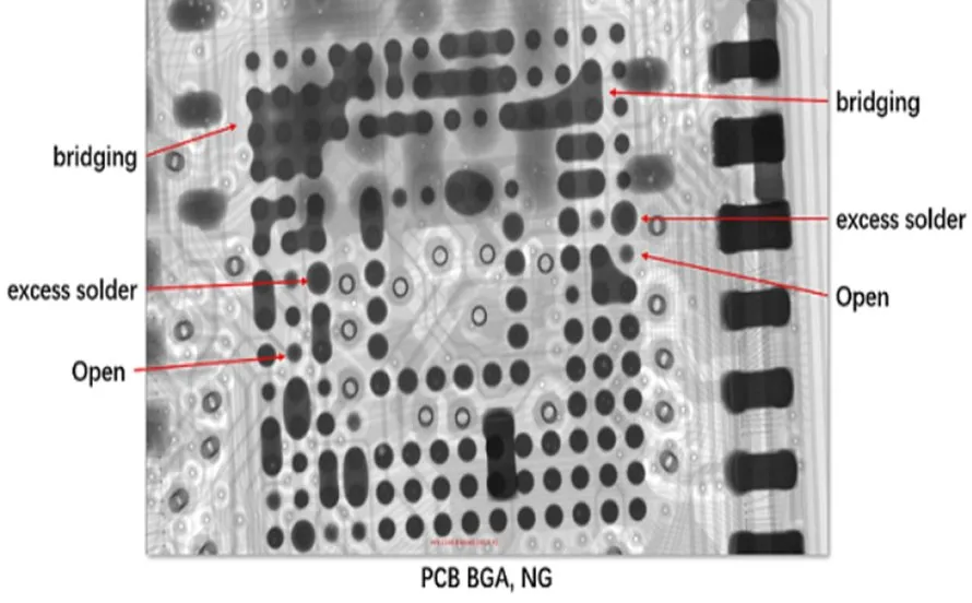
The ultimate objective of X-ray inspection is the precise identification of defects. Here are several common issues to look for and their characteristic appearances in X-ray images:
● Solder Voids: These manifest as lighter, often circular or irregular, spots within the darker solder joints. Voids larger than 20-25% of the joint's cross-sectional area can severely compromise connection strength, escalating the risk of failure, particularly under thermal cycling stress.
● Broken Traces: These appear as distinct gaps or discontinuities in the dark lines that represent copper traces. Even a minute break can disrupt signal integrity, leading to complete circuit failure.
● Misaligned Components: These are visible when a component does not correctly align with its corresponding solder pads. For BGAs, this typically involves solder balls being noticeably offset from their intended grid pattern.
● Insufficient Solder: This condition presents as thinner or less dense dark areas within solder joints. It can result in poor electrical conductivity, potentially causing the resistance values in affected areas to rise above 0.1 ohms.
● Bridging (Solder Bridges): This appears as dark lines or continuous regions connecting two or more adjacent solder points that should be separate. Solder bridging inevitably leads to short circuits, especially problematic in high-density board designs.
It is crucial to meticulously document any identified defects, noting their exact location and assessed severity. This data is critical for informed decisions regarding whether a board requires rework or can proceed to the next stage of assembly. Defect identification is a skill that improves significantly with experience; start with simpler boards and progressively move towards more complex designs.
The Unmatched Benefits of PCB X-ray Inspection for Quality Control
Having thoroughly understood the inspection process, let's underscore why PCB X-ray inspection is a transformative tool for quality control. Firstly, it uncovers defects that alternative methods entirely miss. For example, Automated Optical Inspection (AOI) cannot detect internal solder issues, whereas X-ray inspection reveals them with an accuracy of up to 95% in controlled testing environments. Secondly, the method is non-destructive, meaning the board remains intact and functional after inspection. Lastly, it offers significant time and cost savings by identifying issues early in the production cycle—rework costs can be slashed by 30-50% when defects are caught before final PCBA assembly.
For beginners, integrating X-ray inspection into your workflow ensures that your products consistently meet the highest reliability standards. This is especially vital in industries such as automotive or aerospace, where failure rates must be maintained below 0.01%.
Common Challenges and Practical Tips for Beginner Inspectors
As with any new technical skill, PCB X-ray inspection presents its own set of challenges. Here are some common hurdles and effective strategies to overcome them:
● Blurry Images: This often stems from incorrect system settings or movement during image capture. To remedy this, meticulously double-check the voltage and exposure time settings, and ensure the PCB is absolutely secure on the sample stage.
● Misinterpreting Defects: Novice inspectors might inadvertently confuse normal manufacturing variations with genuine defects. To build confidence and accuracy, routinely cross-reference your images with those from known good samples.
● Equipment Cost: High-end X-ray inspection systems represent a substantial capital investment. However, many specialized service providers offer X-ray inspection as a contracted service, allowing manufacturers to access this technology without the significant upfront cost.
● Safety Concerns: Given the use of radiation, adhering to safety protocols is non-negotiable. Always ensure that all operators receive proper training and strictly follow established safety guidelines.
Patience and consistent practice are paramount to mastering PCB X-ray inspection. Begin with simpler boards, concentrate on solidifying the fundamental techniques, and gradually progress to more complex inspection tasks as your experience and confidence grow.
Conclusion: Achieving Proficiency in PCB X-ray Inspection as a Beginner
PCB X-ray inspection is an indispensable technology for guaranteeing the quality and reliability of printed circuit boards, a necessity that grows with the increasing complexity of modern designs. By diligently following this step-by-step guide, you have acquired a foundational understanding of X-ray basics, proper equipment setup, effective image capture, astute image interpretation, and precise defect identification. This comprehensive PCB X-ray inspection tutorial is specifically crafted to equip beginners with a strong theoretical and practical basis, thereby paving the way for more advanced applications in quality control.
Integrating X-ray inspection into your manufacturing process can lead to a significant reduction in failure rates and a marked improvement in overall product performance. With dedicated practice, you will develop the expertise to identify even the most subtle defects, ensuring that your PCBs consistently adhere to the most rigorous industry standards. Continue your learning journey, maintain consistency in your approach, and harness the immense power of this technology to elevate your manufacturing processes to new heights.