Introduction
Flex PCBs have revolutionized wearable devices by enabling compact, lightweight designs that conform to the human body. In these applications, microvias play a critical role in achieving high-density interconnects without compromising flexibility. Flex PCB microvias allow engineers to route signals efficiently in limited spaces, supporting sensors, processors, and batteries in smartwatches, fitness trackers, and medical wearables. However, designing these structures demands careful consideration of mechanical stresses from repeated bending and twisting. This article explores flexible circuit microvia design principles, reliability challenges, and best practices tailored for electric engineers working on HDI flex PCBs. By understanding these elements, designers can balance density, performance, and durability effectively.
What Are Flex PCB Microvias and Why Do They Matter for Wearables?
Flex PCB microvias are small, blind vias typically formed by laser drilling through thin dielectric layers in flexible substrates like polyimide. According to industry definitions, they feature a maximum aspect ratio of 1:1 and limited depth to ensure reliable plating and minimal stress concentration. In wearable devices, microvia applications wearables become essential due to space constraints, where traditional through-holes would add unnecessary bulk and rigidity. These vias enable HDI flex PCB architectures, allowing multiple layers of fine-pitch traces to interconnect components densely. Without microvias, achieving the miniaturization required for devices like continuous glucose monitors or augmented reality glasses would be impractical. Their integration supports higher component counts while preserving the bendability critical for user comfort and device functionality.
The relevance stems from the unique demands of wearables, which undergo dynamic flexing during daily activities. Microvias must withstand millions of bend cycles without cracking or opening circuits. Poor design can lead to failures like via barrel cracks under thermal expansion mismatch between copper and the flexible dielectric. Engineers prioritize microvias to reduce overall board thickness, improving conformal fitting to curved surfaces such as wrists or heads. This technology also enhances signal integrity for high-speed data from biometric sensors. Ultimately, flex PCB microvias bridge the gap between rigid HDI performance and flexible form factors.
Technical Principles of Microvia Formation in Flexible Circuits
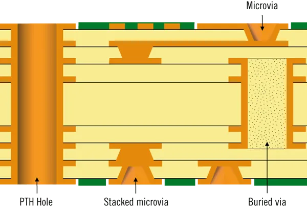
Laser ablation forms the core of flexible circuit microvia design, using UV or CO2 lasers to vaporize dielectric material precisely without damaging adjacent copper. The process creates a conical or straight barrel, optimizing plating adhesion and resin flow during via fill. In flex materials, polyimide's thermal stability resists charring, but engineers must select laser parameters to match the substrate's ablation threshold. Aspect ratios stay below 1:1 to prevent plating voids, with capture and target pads oversized relative to the via diameter for stress relief. These principles ensure interconnections survive the sequential lamination builds common in HDI flex PCBs.
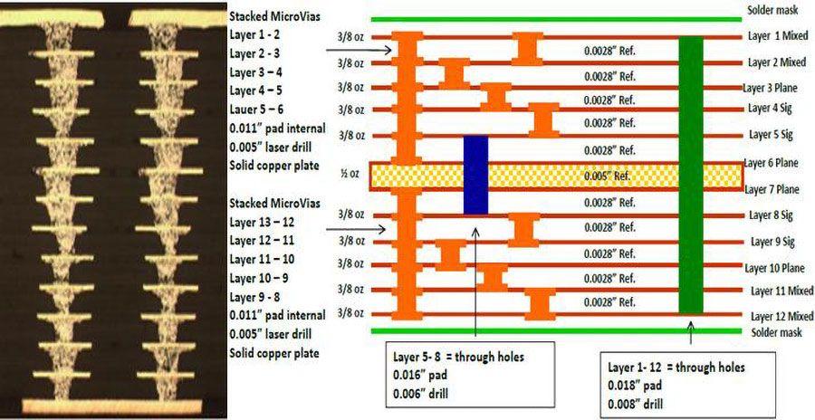
Stackup configuration influences microvia placement significantly. Single-level microvias suit simple flex designs, connecting outer layers to inner traces without penetrating the entire board. Staggered arrangements distribute stress better than stacked vias, avoiding cumulative fatigue in bend zones. In HDI flex PCB builds, engineers offset vias vertically by at least the via diameter to minimize inter-via interaction during flexing. Copper fill or conductive epoxy reinforces vias against shear forces from repeated deformation. Thermal expansion differences between copper foil and polyimide necessitate controlled lamination pressures to avoid delamination at via interfaces.
Bend radius constraints dictate microvia exclusion from high-strain areas. IPC-2223 provides guidelines for conductor spacing and hole-to-edge clearances in flexible sections, ensuring vias reside in rigid or transition zones. Dynamic bending induces tensile and compressive strains, potentially cracking plated barrels if vias align perpendicular to the bend axis. Engineers model strain distribution using finite element analysis to position microvias optimally. Adhesive layers between flex and coverlay must accommodate via protrusions without air entrapment. These mechanisms collectively define robust flexible circuit microvia design.
Best Practices for Microvia Reliability in Flex Circuits
Adhering to established design rules forms the foundation of microvia reliability flex circuits. Maintain via diameters between 75-150 microns, with pad sizes at least 1.5 times larger to distribute mechanical loads. Prefer blind microvias over through-vias in flex tails to preserve flexibility, and incorporate teardrop entries for trace-to-pad transitions reducing stress risers. During layout, route high-current paths away from microvias to limit Joule heating, which exacerbates fatigue in polyimide. Simulate bending cycles early to validate via survival under expected radii, typically 1-3 mm for wearables.
Material selection critically impacts HDI flex PCB performance. Choose low-elongation polyimides with uniform glass transition temperatures for consistent laser drilling. Coverlay and bondply thickness uniformity prevents warpage during thermal excursions. Via plating thickness should meet minimum copper weights, electroplated after desmear to ensure barrel integrity. Post-plating anneal relieves hydrogen embrittlement, enhancing ductility for flex applications. These practices mitigate common failures like pad lift-off or resin cracking.
Testing protocols verify design robustness before production. Conduct bend fatigue tests per IPC-6013 qualification schemes, cycling boards to simulate wearable motions. Thermal shock from -40°C to 125°C exposes CTE mismatch issues at via sites. Electrical continuity monitoring during flexing detects incipient opens. Cross-section analysis reveals plating quality and fill density. Implementing these steps ensures microvias endure real-world stresses.
Challenges and Solutions in Microvia Applications for Wearables
Wearables impose unique challenges on flex PCB microvias due to conformal shaping and moisture exposure. Sweat and skin contact accelerate corrosion if vias lack proper encapsulation. Solutions include selective coverlay over vias and conformal coatings for hermetic sealing. Multi-axis flexing in devices like smart rings demands vias oriented parallel to primary bend planes. Engineers employ strain-relief patterns, such as serpentine traces, adjacent to microvia fields.
Reliability data from accelerated life testing guides iterations. Stacked microvias, while density-enabling, accumulate stress faster than staggered in flex environments. IPC-2226 outlines HDI build types, recommending Type II or III configurations with offset vias for flex hybrids. Finite pitch BGAs in wearables benefit from via-in-pad designs, capped to prevent solder wicking. Fabrication notes specify laser type and plating chemistry for reproducibility.
Integration with rigid sections in rigid-flex hybrids requires transition zone optimization. Microvias bridge flex-to-rigid interfaces, but fiducials ensure alignment during lamination. Avoiding vias in stiffener overlaps prevents rigidity propagation into flex areas. These targeted solutions enhance overall system reliability.
Practical Implementation in Wearable Device Design
In practice, engineers start with stackup planning for HDI flex PCB prototypes. Define microvia layers based on BGA escape routing needs, prioritizing outer-layer access for sensors. Gerber files include drill charts distinguishing laser from mechanical holes. DFM reviews flag via clusters exceeding density rules. Pilot builds incorporate test coupons for via chain continuity.
Assembly considerations influence microvia design. Reflow profiles must avoid peak temperatures exceeding polyimide limits, preventing via cratering. Underfill or edge bonding secures components against peel forces. Field data from wearables informs iterative improvements, such as widening pads in high-humidity zones. Collaborative design-fabrication loops accelerate reliability gains.
Conclusion
Microvia design for flex PCBs demands a holistic approach integrating mechanical, thermal, and electrical principles. Flex PCB microvias enable the high-density, flexible interconnects essential for wearable innovation while upholding reliability. By following structured guidelines, selecting appropriate materials, and rigorous testing, engineers achieve durable HDI flex PCB solutions. Key takeaways include prioritizing staggered vias, respecting bend constraints, and leveraging standards like IPC-2223, IPC-6013, and IPC-2226. These practices ensure wearables perform reliably in dynamic environments, paving the way for next-generation devices.
FAQs
Q1: What are the key design rules for flex PCB microvias in HDI applications?
A1: Flexible circuit microvia design requires aspect ratios below 1:1, with diameters under 150 microns and oversized pads for stress relief. Position vias away from bend radii per IPC-2223 guidelines to avoid fatigue. Use laser-drillable polyimides and staggered configurations for optimal density. Simulate strains and include test coupons to validate reliability before scaling production.
Q2: How does microvia reliability flex circuits impact wearable performance?
A2: Microvia reliability flex circuits determines longevity under bending and thermal cycling in wearables. Failures like barrel cracks disrupt sensor signals, leading to data loss. Robust plating and fill enhance cycle life, supporting millions of flexes. Standards like IPC-6013 qualification tests confirm endurance matching device lifecycles.
Q3: What role do microvia applications wearables play in miniaturization?
A3: Microvia applications wearables enable HDI flex PCB stackups for compact sensor arrays and processors. They reduce layer count and thickness, allowing conformal device shapes. Stacked or staggered vias route fine-pitch components efficiently. This supports battery optimization and comfort in fitness trackers or hearables.
Q4: Why choose HDI flex PCB for wearable prototypes?
A4: HDI flex PCB offers high interconnect density with flexibility, ideal for prototyping wearables. Microvias facilitate quick iterations on dense layouts. Reliability testing per industry standards ensures production viability. Engineers gain performance akin to rigid boards in bendable formats.
References
IPC-6013D - Qualification and Performance Specification for Flexible/Rigid-Flexible Printed Boards. IPC
IPC-2226A - Sectional Design Standard for High Density Interconnect (HDI) Printed Boards. IPC, 2017
IPC-2223E - Sectional Design Standard for Flexible/Rigid-Flexible Printed Boards. IPC


