Introduction
Electronics continue to evolve toward smaller, more powerful devices, driven by demands from consumer gadgets, medical implants, and autonomous systems. High-Density Interconnect (HDI) PCB technology stands at the forefront of this miniaturization trend, enabling unprecedented component density and performance in compact form factors. Engineers face constant pressure to pack more functionality into less space while maintaining reliability and signal integrity. HDI PCBs achieve this through advanced features like microvias and multilayer build-ups, which outperform traditional designs in high-density interconnect applications. As devices shrink further, understanding HDI principles becomes essential for electric engineers tackling next-generation projects. This article explores the core elements of HDI technology, from design to manufacturing, to guide informed decision-making.
What Is HDI PCB Technology and Why It Matters
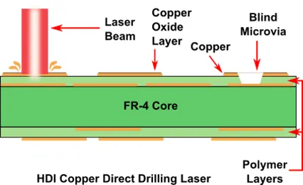
HDI PCB technology refers to printed circuit boards that incorporate finer lines, smaller vias, and additional layers to maximize interconnect density compared to standard multilayer boards. These boards use microvias, typically drilled with lasers for precision, allowing connections between adjacent layers without penetrating the entire stack. The result is reduced board size, shorter signal paths, and improved electrical performance, critical for modern electronics. In an industry where space constraints define feasibility, HDI technology matters because it supports the integration of high-pin-count components like BGAs and CSPs. Electric engineers rely on it for applications requiring compactness without sacrificing functionality. Ultimately, HDI drives innovation by aligning with the shrinking footprints of semiconductors and modules.
Core Technical Principles of HDI PCBs
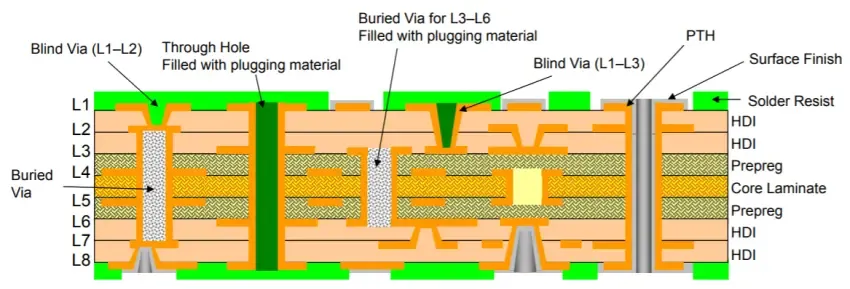
HDI PCBs build on conventional multilayer construction but introduce sequential layering and specialized vias to achieve higher densities. Microvias connect only two or three layers, minimizing board thickness and enabling tighter layouts. These vias undergo laser ablation followed by plating or filling to ensure robust electrical and mechanical properties. The stack-up configuration in HDI PCBs often involves a central core surrounded by build-up layers, where each addition refines interconnect capabilities. Sequential lamination PCB processes allow for staggered via formations, preventing alignment issues across multiple levels. This layered approach reduces parasitic inductance and capacitance, enhancing high-speed signal propagation.
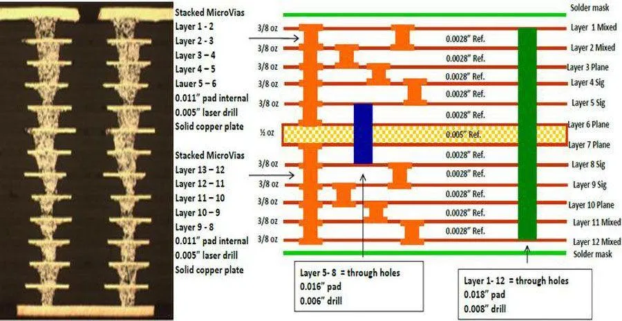
HDI stack-ups are classified by via configurations, such as 1+n+1 for simple build-ups or more complex 2+n+2 setups with staggered microvias. Engineers must consider material selection for dielectric layers to match CTE values and prevent delamination during thermal cycling. Copper foil thickness decreases in outer layers to support finer features, while inner layers handle power distribution. Reliability hinges on controlling via aspect ratios and plating uniformity throughout the build. Adherence to standards like IPC-6016 ensures qualification for demanding environments. These principles collectively enable HDI to outperform standard boards in density and efficiency.
HDI PCB Design Rules: Foundations for Success
HDI PCB design rules dictate minimum line widths, spaces, and via dimensions to ensure manufacturability and performance. Engineers start by defining pad sizes and clearances around microvias, accounting for laser drilling tolerances and plating growth. Aspect ratios for vias remain conservative to facilitate plating chemistry penetration, avoiding voids or cracking. Sequential lamination PCB designs require planning lamination cycles upfront, specifying which layers bond sequentially to stack vias properly. Signal integrity rules incorporate length matching and impedance control for high-density interconnect applications. Fanout strategies from fine-pitch components leverage microvias to escape signals efficiently without expanding board outlines.
Design flows emphasize simulation for thermal and mechanical stresses, as HDI stack-ups amplify warpage risks from CTE mismatches. Rules also cover annular ring sizes to prevent via breakout during fabrication. Electric engineers iterate designs using stack-up calculators to optimize layer count and thickness. Compliance with IPC-2226 guidelines standardizes these rules across projects. Proactive rule adherence minimizes iterations and accelerates time-to-market. Mastering these rules unlocks the full potential of HDI for miniaturized systems.
Microvia PCB Manufacturing: Precision in Every Step
Microvia PCB manufacturing begins with core fabrication, followed by sequential build-up of dielectric and copper layers. Laser drilling creates precise microvia holes in photosensitive dielectrics, targeting locations defined by design files. Subsequent desmear processes clean residues, preparing surfaces for electroless copper seeding and electroplating. Via filling options, such as conductive paste or electroplated copper, provide planar surfaces for next-layer lamination. Sequential lamination PCB techniques involve multiple press cycles, with temporary carriers to maintain flatness during partial builds. Final outer layer patterning uses advanced imaging for sub-50-micron features.
Quality control inspects via integrity through cross-sectioning and electrical testing, verifying continuity and resistance. Solder mask application protects fine traces, while surface finishes enhance solderability. Manufacturing yields improve with controlled process parameters, like resin flow during lamination to avoid voids. IPC-A-600 criteria guide acceptability inspections for surface and internal features. Engineers benefit from understanding these steps to select partners capable of consistent HDI production. This precision manufacturing scales high-density interconnect applications reliably.
High-Density Interconnect Applications: Real-World Impact
High-density interconnect applications span consumer electronics, where HDI PCBs fit processors and memory into slim smartphones and wearables. In automotive radar modules, they manage multi-gigabit data rates over short paths, reducing EMI. Medical devices like pacemakers leverage HDI for battery-efficient, compact designs with integrated sensors. Aerospace avionics demand HDI for rugged, high-reliability interconnects in vibration-prone environments. Telecommunications gear uses stacked microvias to consolidate RF and baseband functions. These applications highlight HDI's versatility in pushing miniaturization boundaries.
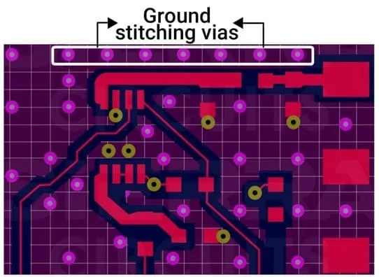
Challenges in applications include managing power delivery in dense layouts and ensuring thermal dissipation from crowded components. HDI stack-ups incorporate embedded planes for low-impedance power distribution. Sequential lamination PCB enables customized builds for specific thermal profiles. Engineers troubleshoot signal crosstalk using shielding vias and ground stitching. Long-term reliability testing simulates field conditions, confirming performance. HDI technology thus shrinks electronics while elevating functionality across sectors.
Best Practices for HDI Implementation
Electric engineers should prioritize symmetric HDI PCB stack-ups to mitigate warpage from asymmetric build-ups. Balance copper distribution across layers to equalize stresses during lamination and reflow. Select low-loss dielectrics for high-frequency high-density interconnect applications, verifying Dk and Df values early. Simulate via thermal reliability to predict electromigration risks under current loads. Establish design reviews focusing on microvia fanout and escape routing density. Partner with fabricators experienced in sequential lamination PCB for process feedback.
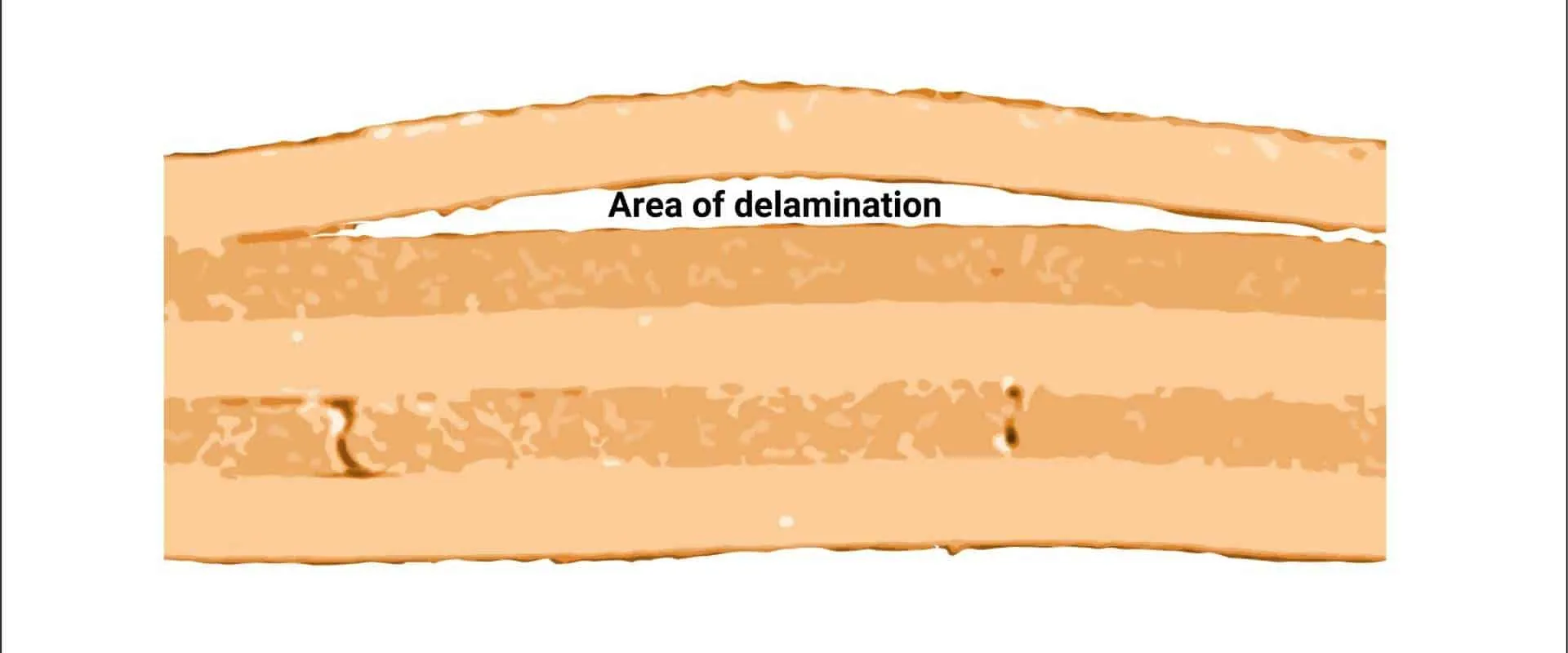
In prototyping, limit initial builds to simpler 1+n+1 configurations before scaling complexity. Monitor plating bath chemistry for uniform via fill, preventing reliability failures. Post-fabrication, perform scanning acoustic microscopy to detect delaminations. Document HDI PCB design rules in PDKs for team consistency. These practices ensure robust, manufacturable designs. Continuous refinement based on test data refines future iterations.
Conclusion
HDI PCB technology masters miniaturization by integrating microvias, advanced stack-ups, and sequential processes into compact, high-performance boards. From HDI PCB design rules to microvia PCB manufacturing, each element contributes to denser, faster electronics. Electric engineers gain a competitive edge by applying these principles thoughtfully, balancing density with reliability. As demands for smaller devices intensify, HDI remains pivotal for innovation. Embracing its standards and best practices positions teams to shrink the future effectively.
FAQs
Q1: What are the key HDI PCB design rules for electric engineers?
A1: HDI PCB design rules emphasize minimum trace widths, via pad sizes, and clearances tailored to microvia tolerances. Engineers define aspect ratios conservatively for plating reliability and plan sequential via stacking to avoid misalignment. Impedance control and fanout strategies ensure signal integrity in dense layouts. Compliance with IPC-2226 standardizes these rules, reducing fabrication risks and iterations. Overall, structured rule sets enable efficient high-density interconnect applications.
Q2: How does microvia PCB manufacturing differ from standard processes?
A2: Microvia PCB manufacturing uses laser drilling for precise, small-diameter holes in build-up dielectrics, followed by plating or filling. Sequential lamination bonds layers incrementally, supporting stacked configurations unlike all-at-once pressing in standard boards. Desmear and plating steps ensure void-free vias for reliability. IPC-6016 qualifications verify performance under stress. This process achieves finer features essential for miniaturization.
Q3: What role does HDI PCB stack-up play in high-density interconnect applications?
A3: HDI PCB stack-up determines layer sequencing, via staggering, and thickness control, directly impacting density and signal paths. Core-plus-build-up designs shorten interconnects, reducing latency in applications like wearables and radar. Symmetric configurations minimize warpage during thermal excursions. Engineers optimize for CTE matching and power planes. Proper stack-up unlocks compact, high-performance electronics.
Q4: Why is sequential lamination PCB critical for advanced HDI builds?
A4: Sequential lamination PCB allows staggered microvia placement across multiple levels, enabling complex 2+n+2 or higher configurations. It involves phased pressing with carriers for flatness, preventing defects in dense stacks. This method supports microvia stacking without full penetration, ideal for high-density interconnect applications. Reliability improves as each lamination cycle refines interlayer bonds. It expands design flexibility for shrinking devices.
References
IPC-6016F — Qualification and Performance Specification for High Density Interconnect (HDI) Printed Boards. IPC, 2022
IPC-2226B — Design Standard for High Density Interconnect (HDI) Layer 1 and Layer 2. IPC, 2021
IPC-A-600M — Acceptability of Printed Boards. IPC, 2020