Introduction
High-frequency PCBs operate at signal speeds exceeding several gigahertz, where even minor losses can degrade performance significantly. Signal loss in these designs manifests as insertion loss, which reduces signal amplitude over distance and compromises data integrity. Engineers face challenges from conductor and dielectric contributions that intensify with frequency. This comprehensive guide explores the mechanisms behind high-frequency signal loss and provides structured strategies to minimize it. By understanding skin effect, copper roughness, and dielectric loss, designers can optimize PCB layouts for reliable operation in demanding applications. Adhering to established principles ensures compliance with performance expectations.
Understanding Signal Loss in High-Frequency PCBs
Signal loss refers to the attenuation of electrical signals as they propagate through PCB traces and dielectrics. In high-frequency environments, insertion loss becomes the primary metric, quantifying total power loss from input to output. This loss arises from resistive heating in conductors and energy dissipation in insulating materials. Why does it matter? Excessive high-frequency signal loss leads to bit errors, reduced eye diagram margins, and failure to meet timing budgets in high-speed serial links. Engineers must prioritize minimization to support rising data rates in telecommunications and computing systems. Proper management maintains signal integrity across the entire channel.
Key Mechanisms Causing High-Frequency Signal Loss
The Skin Effect
The skin effect confines alternating current to the outer surface of conductors as frequency increases. At high frequencies, current density drops exponentially toward the conductor center, raising effective resistance. This phenomenon directly contributes to conductor loss within insertion loss. Trace width and thickness influence the severity, with thinner conductors exacerbating the issue. Engineers observe this in time-domain reflectometry, where reflections indicate increased attenuation. Mitigating skin effect requires adjustments in trace geometry and surface properties.
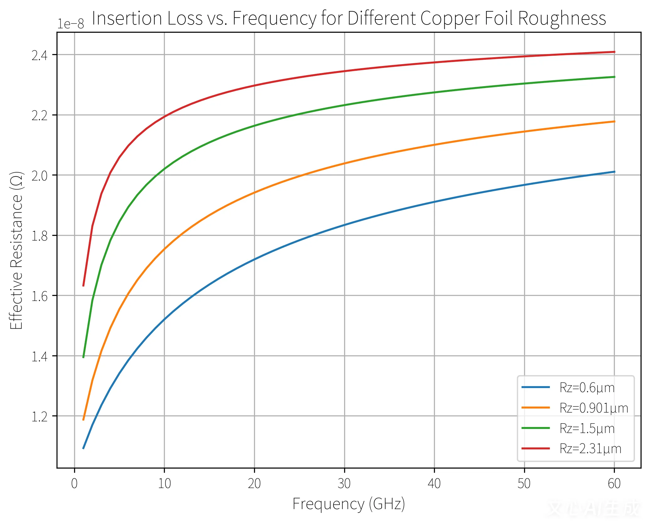
Copper Roughness Impact
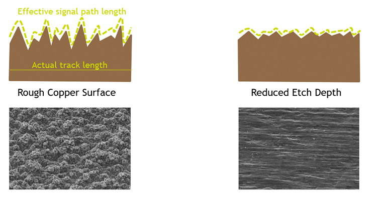
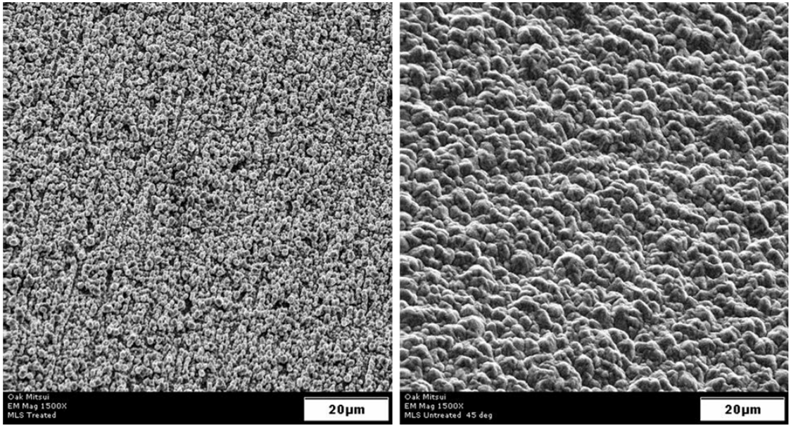
Copper roughness on PCB traces scatters high-frequency currents, increasing path length and resistive losses. Rough surfaces trap fields within peaks and valleys, amplifying skin effect consequences. This roughness, often from manufacturing electrodeposition, becomes prominent above 1 GHz. Surface profilometry reveals variations that correlate with elevated insertion loss. Smoother profiles reduce scattering and maintain uniform current flow. Balancing adhesion for plating with minimal roughness proves essential for high-frequency signal loss control.
Dielectric Loss Mechanisms
Dielectric loss stems from the dissipation factor of laminate materials, converting signal energy to heat. Polarization losses in the dielectric intensify with frequency and material tan delta. High-frequency signal loss accelerates as dielectric constant and loss tangent interact with trace capacitance. Material homogeneity affects uniformity, with voids or inconsistencies worsening attenuation. Engineers select laminates based on specified Df values at operating frequencies. This loss often dominates over conductor contributions in multilayer stacks.
Practical Strategies to Minimize Signal Loss
Material Selection for Low Loss
Choosing laminates with low dielectric constant and dissipation factor directly curbs dielectric loss. Materials exhibiting stable Df up to 10 GHz or higher support minimal high-frequency signal loss. Engineers evaluate tan delta at relevant frequencies during selection. Hybrid stackups combining low-loss cores with cost-effective prepregs optimize overall performance. IPC-2221 provides guidelines for material considerations in high-speed designs, ensuring compatibility with fabrication processes. Verification through vector network analyzer testing confirms reductions in insertion loss.
Optimizing Conductor Surfaces and Geometry
Low-profile copper foils minimize roughness-induced losses while preserving peel strength. Electrodeposited foils with reverse treated surfaces offer smoother profiles for high-frequency applications. Wider traces or increased copper thickness counteract skin effect by expanding the effective current-carrying area. Rounded trace corners reduce field concentration and scattering compared to sharp bends. Controlled impedance calculations incorporate roughness factors for accurate modeling. These adjustments yield measurable drops in conductor loss contributions.
Stackup and Layout Best Practices
Symmetric stackups prevent warpage and maintain consistent dielectric spacing for impedance control. Positioning high-speed signals on inner layers shields them from external interference while minimizing radiation losses. Reducing via count and stub lengths avoids discontinuities that amplify insertion loss. Differential pair routing with tight length matching preserves balance and reduces common-mode losses. Ground plane proximity enhances return path efficiency, curbing skin effect impacts. IPC-TM-650 test methods guide measurement of these optimizations during qualification.
Fabrication and Processing Considerations
Controlled plating processes limit copper roughness growth during via filling and panelization. Low-etchback profiles preserve smooth surfaces post-patterning. Bake-out procedures remove moisture, stabilizing dielectric properties against loss variations. Solder mask selection with low Df prevents additional surface losses on exposed traces. Post-fabrication annealing can refine grain structure for further smoothness. These steps align with J-STD-001 requirements for high-reliability assemblies.
Troubleshooting High Insertion Loss Issues
Engineers encountering elevated insertion loss first perform time-domain and frequency-domain sweeps to isolate conductor versus dielectric dominance. Excessive skin effect appears as frequency-squared dependence in loss curves. Copper roughness suspicions prompt surface scans and comparison against baseline foils. Dielectric anomalies manifest in temperature-sensitive attenuation shifts. Common fixes include trace redesign or material respinning. Systematic de-embedding of connectors isolates PCB contributions accurately.
Conclusion
Minimizing signal loss in high-frequency PCBs demands a holistic approach targeting skin effect, copper roughness, dielectric loss, and insertion loss holistically. Logical material choices, surface optimizations, and layout discipline yield substantial gains. Standards like IPC-2221 reinforce these practices for reproducible results. Engineers applying these strategies enhance signal integrity across gigahertz bands. Continuous validation through standardized tests ensures long-term reliability. Future designs will leverage advancing materials to push performance boundaries further.
FAQs
Q1: What is the skin effect and its role in high-frequency signal loss?
A1: The skin effect causes AC currents to concentrate on conductor surfaces at high frequencies, increasing effective resistance and contributing to insertion loss. This leads to higher conductor losses as frequency rises. Engineers mitigate it using thicker or wider traces and smooth copper. Proper modeling predicts impact during design phases.
Q2: How does copper roughness affect insertion loss in PCBs?
A2: Copper roughness scatters high-frequency currents, extending effective path lengths and amplifying skin effect losses. Rougher profiles correlate with steeper insertion loss curves above 5 GHz. Smoother foils reduce this by minimizing field trapping. Surface treatment choices balance adhesion and performance needs.
Q3: What strategies reduce dielectric loss for high-frequency signal loss?
A3: Select laminates with low dissipation factor and stable dielectric constant across frequencies. Symmetric stackups ensure uniform fields and minimal polarization losses. Avoid moisture absorption through proper handling. Testing per industry methods verifies improvements in overall insertion loss.
Q4: Why measure insertion loss in high-frequency PCB designs?
A4: Insertion loss quantifies total signal attenuation from all sources, guiding optimizations for skin effect, roughness, and dielectric contributions. It directly impacts eye height and jitter margins. Frequency sweeps reveal dominant mechanisms for targeted fixes. Compliance with design standards confirms adequacy.
References
IPC-2221B — Generic Standard on Printed Board Design. IPC, 2003
IPC-TM-650 — Test Methods Manual. IPC, 2020
IPC-6012E — Qualification and Performance Specification for Rigid Printed Boards. IPC, 2015
J-STD-001H — Requirements for Soldered Electrical and Electronic Assemblies. IPC, 2020


