Introduction
Multilayer printed circuit boards are the backbone of modern electronics, enabling compact and high-performance devices across industries like aerospace, medical, and telecommunications. These boards, with their multiple layers of conductive traces and insulating materials, present unique challenges when damage occurs. Repairing vias in multilayer PCBs, troubleshooting internal shorts, accessing internal traces, and addressing delamination are tasks that demand precision and expertise. For electrical engineers, understanding these challenges and applying advanced techniques for multilayer PCB repair is essential to maintain functionality and reliability. This article explores the complexities of multilayer PCB repair, outlines common issues, and provides practical solutions to ensure successful outcomes while adhering to industry standards.
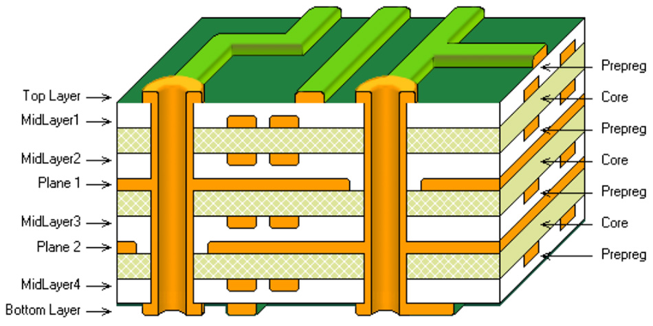
What Are Multilayer PCBs and Why Do They Matter
Multilayer PCBs consist of three or more conductive layers separated by insulating materials, bonded together through lamination. Unlike single or double layer boards, they offer higher circuit density, improved signal integrity, and reduced electromagnetic interference. These attributes make them indispensable in complex applications where space and performance are critical. However, their intricate structure complicates repair processes. Damage to internal layers or vias can disrupt functionality, and without proper techniques, repairs may compromise the board’s reliability. For electrical engineers, mastering multilayer PCB repair ensures minimal downtime and preserves the integrity of critical systems, aligning with stringent quality requirements in high stakes environments.
Challenges in Multilayer PCB Repair
Complexity of Internal Structures
The primary challenge in multilayer PCB repair lies in the hidden nature of internal layers. Unlike surface issues, damage such as internal shorts or broken traces is not visible, making diagnosis and access difficult. Electrical engineers must rely on specialized tools and methods to locate faults without causing further harm to the board. The risk of damaging adjacent layers during repair adds another layer of complexity, requiring precise control over every step of the process.
Issues with Vias and Interconnections
Vias, which connect different layers of a multilayer PCB, are prone to damage during manufacturing or operation. Cracks, plating defects, or mechanical stress can disrupt connectivity. Repairing vias in multilayer PCBs demands meticulous attention to restore conductivity without affecting surrounding areas. Faulty vias can lead to signal loss or complete circuit failure, making this a critical area of focus for repair efforts.
Internal Shorts and Their Detection
Troubleshooting internal shorts in multilayer PCBs is a daunting task due to the inaccessibility of inner layers. Shorts often result from manufacturing defects, excessive heat, or physical stress, causing unintended connections between layers. Identifying the exact location of a short without destructive testing requires advanced diagnostic tools and a deep understanding of circuit behavior. Failure to address shorts can lead to overheating or component damage.
Accessing Internal Traces for Repair
Accessing internal traces in multilayer PCBs poses a significant hurdle. Since these traces are embedded within the board, reaching them often involves removing outer layers or drilling, which risks further damage. Engineers must balance the need for access with the preservation of the board’s structural integrity. This process demands both skill and patience to avoid compromising the entire assembly.
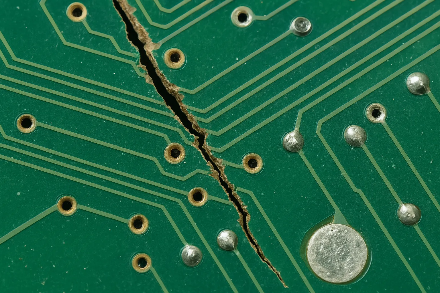
Delamination and Structural Integrity
Delamination, the separation of layers within a multilayer PCB, often occurs due to thermal stress, moisture, or poor manufacturing practices. This defect weakens the board’s structure and can disrupt electrical connections. Delamination repair in multilayer PCBs requires careful application of heat and pressure to rebond layers, a process that must be executed with precision to prevent additional issues.
Related Reading: PCB Repair and Common issues: How to resolve
Technical Causes of Multilayer PCB Damage
Thermal and Mechanical Stress
Multilayer PCBs are sensitive to thermal expansion and mechanical stress. During operation, components generate heat, causing materials to expand at different rates. This mismatch can lead to cracks in vias or delamination between layers. Similarly, physical handling or vibration can fracture internal traces or weaken solder joints. Understanding these stress factors is crucial for engineers to predict potential failure points and implement effective repairs.
Manufacturing Defects
Even with strict quality controls, manufacturing defects can introduce flaws in multilayer PCBs. Incomplete plating of vias, improper lamination, or contamination during production can create weak points that manifest as failures over time. These defects often remain hidden until operational issues arise, complicating the repair process. Standards such as IPC-6012E provide guidelines for identifying acceptable quality levels and addressing such issues during inspection and repair.
Environmental Factors
Exposure to moisture, humidity, or corrosive environments can degrade multilayer PCBs. Moisture ingress may cause delamination or corrosion of internal traces, while extreme temperatures can exacerbate thermal stress. Engineers must consider these factors when diagnosing damage and selecting repair methods to ensure long term reliability in challenging conditions.
Practical Solutions for Multilayer PCB Repair
Repairing Vias in Multilayer PCBs
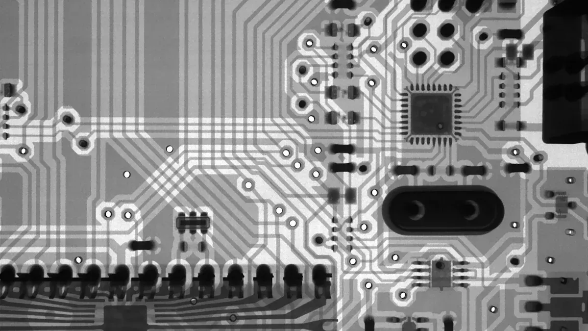
To repair vias, engineers first assess the extent of damage using continuity testing or X-ray inspection to confirm breaks or plating issues. If the via is salvageable, a conductive epoxy or micro soldering can restore connectivity. For severely damaged vias, drilling out the old via and inserting a replacement conductor may be necessary. Precision is key to avoid affecting adjacent layers, and adherence to standards like IPC-A-600K ensures acceptable repair quality.
Related Reading: How to Repair Damaged Plated Through-Holes (PTH) on a PCB
Troubleshooting Internal Shorts in Multilayer PCBs
Identifying internal shorts often begins with thermal imaging to detect heat anomalies indicating a fault. Once located, engineers use controlled current injection to pinpoint the short without causing further damage. If the short is accessible, micro cutting tools can isolate the affected area. For deeper issues, partial delayering may be required, though this should be a last resort due to the risk of structural compromise.
Accessing Internal Traces in Multilayer PCBs
Accessing internal traces requires careful planning to minimize damage. Engineers can use micro drilling or laser ablation to reach the target layer, guided by X-ray or schematic analysis. Once accessed, damaged traces are repaired using fine gauge wire or conductive ink, ensuring proper insulation to prevent future shorts. This process demands steady hands and specialized equipment to maintain the board’s integrity.
Delamination Repair in Multilayer PCBs
Delamination repair involves applying controlled heat and pressure to rebond separated layers. Engineers clean the affected area to remove contaminants, then use a press with precise temperature control to re laminate the board. Epoxy resins may be injected into small gaps to reinforce bonding. Following guidelines from IPC-6012E ensures that repaired boards meet performance and reliability standards after the process.
Advanced Techniques for Multilayer PCB Repair
Advanced techniques for multilayer PCB repair include the use of automated optical inspection for fault detection and micro robotic tools for precise soldering or cutting. X-ray laminography provides detailed imaging of internal structures without destructive testing. Additionally, conductive ink printing can rebuild damaged traces with high accuracy. These methods, while resource intensive, offer superior results for complex repairs in high reliability applications.
Best Practices for Successful Repairs
- Always start with non destructive testing methods to diagnose issues.
- Use calibrated tools to ensure precision during micro soldering or drilling.
- Document every step of the repair process for traceability and future reference.
- Adhere to industry standards like IPC-A-600K for acceptability criteria.
- Test the repaired board under simulated operating conditions to verify functionality.
Troubleshooting Insights for Electrical Engineers
When tackling multilayer PCB repair, prioritize a systematic approach to troubleshooting. Begin with a thorough visual inspection under magnification to spot surface anomalies. Move to electrical testing for continuity and resistance measurements, isolating problematic areas. For internal issues, integrate imaging technologies to visualize hidden defects. A common pitfall is rushing into invasive repairs without adequate diagnosis, which can exacerbate damage. Instead, allocate time for detailed analysis, ensuring that each intervention is justified and aligned with standards like IPC-6012E. Post repair testing is non negotiable, as it confirms the board’s readiness for real world conditions.
Conclusion
Multilayer PCB repair presents significant challenges due to the intricate design and hidden nature of internal components. Issues like damaged vias, internal shorts, inaccessible traces, and delamination require a blend of technical knowledge and practical skills to address effectively. By employing advanced techniques for multilayer PCB repair and adhering to established industry standards, electrical engineers can restore functionality and reliability to complex circuit boards. Understanding the root causes of damage and applying targeted solutions ensures minimal disruption and long term performance. As technology evolves, staying updated on repair methodologies remains critical for success in this demanding field.
FAQs
Q1: What are the main challenges in repairing vias in multilayer PCBs?
A1: Repairing vias in multilayer PCBs is challenging due to their small size and location within internal layers. Damage like cracks or plating defects can disrupt connectivity, requiring precise tools for diagnosis and repair. Engineers often use X-ray inspection to locate issues and micro soldering to restore conductivity, ensuring minimal impact on surrounding areas while adhering to industry standards for quality.
Q2: How can I troubleshoot internal shorts in multilayer PCBs effectively?
A2: Troubleshooting internal shorts in multilayer PCBs involves using thermal imaging to detect heat anomalies and controlled current injection to pinpoint the fault. Non destructive methods are preferred to avoid further damage. Once identified, isolating the short with micro cutting tools or partial delayering may be necessary, followed by thorough testing to confirm resolution of the issue.
Q3: What advanced techniques for multilayer PCB repair should engineers consider?
A3: Advanced techniques for multilayer PCB repair include X-ray laminography for detailed internal imaging, micro robotic tools for precise interventions, and conductive ink printing for trace reconstruction. Automated optical inspection aids in fault detection with high accuracy. These methods enhance repair outcomes for complex boards, especially in high reliability applications where precision is paramount.
Q4: How is delamination repair in multilayer PCBs performed?
A4: Delamination repair in multilayer PCBs involves cleaning the affected area to remove contaminants, then applying controlled heat and pressure to rebond layers. Epoxy resins may be used for reinforcement in small gaps. Precision in temperature control is critical to avoid further damage, and adherence to standards ensures the repaired board meets reliability requirements for continued use.
References
IPC-6012E — Qualification and Performance Specification for Rigid Printed Boards. IPC, 2020.
IPC-A-600K — Acceptability of Printed Boards. IPC, 2020.


