Why Does Breakaway Tab Placement Matter in PCB Design?
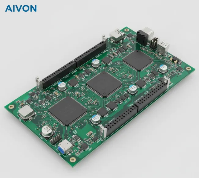
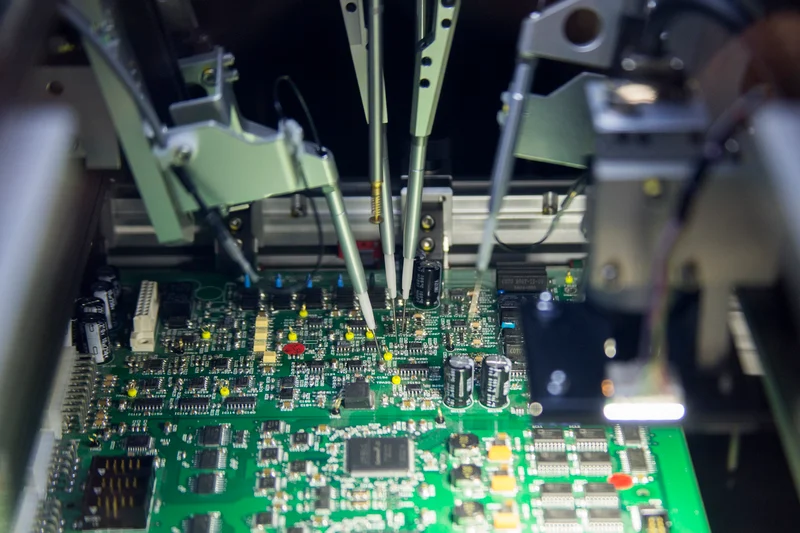
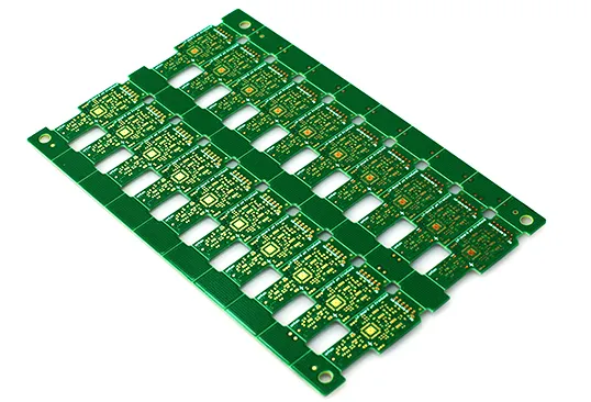
Breakaway tabs, often referred to as mouse bites, are crucial for modern PCB manufacturing. These small connectors integrate individual circuit boards into a larger panel, streamlining the production and assembly process. Their primary role is to hold boards securely during automated assembly and then allow for clean separation, or depanelization, once manufacturing is complete.
However, the placement of these tabs is more critical than often perceived. Suboptimal positioning can lead to uneven stress distribution during depanelization, potentially causing issues like board flexing, cracks, delamination, or even failure of sensitive components. Strategic tab placement is key to minimizing stress and ensuring a smooth, damage-free separation process.
What Causes Stress During PCB Depanelization?
The process of separating individual PCBs from a panel introduces mechanical stress, particularly concentrated around the breakaway tabs. This stress, if not managed correctly, can propagate through the board, potentially compromising traces, solder joints, or mounted components. Several factors contribute to the level of stress experienced by the PCB during this critical phase.
Factors Influencing Depanelization Stress
The location of breakaway tabs significantly impacts stress distribution; placing them too close to delicate components or thin board sections can create vulnerable hotspots. The specific design of the tab, including the number and size of perforations, dictates the force required for a clean break, directly influencing stress levels. Furthermore, the inherent properties of the board material, such as the tensile strength of FR-4 (typically around 310 MPa), determine its capacity to withstand stress before structural integrity is compromised. Performing a thorough breakaway tab stress analysis can help identify and mitigate these risks proactively.
What Are the Best Strategies for Reducing PCB Depanelization Stress?
Achieving effective PCB depanelization stress reduction requires a thoughtful combination of design principles and precise planning. Integrating these actionable strategies into your design process can significantly enhance board reliability and manufacturing yield.
Strategic Tab Positioning
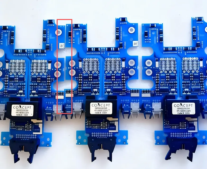
Place breakaway tabs thoughtfully, keeping them clear of high-stress zones such as board corners or areas with dense component layouts. The ideal approach is to position tabs along the board's edges where the material offers greater thickness and inherent rigidity, reducing the likelihood of excessive flexing. For instance, centering tabs along each side rather than at the corners promotes more even stress distribution. A general guideline suggests maintaining a minimum clearance of 5 mm from any critical components or mounting holes to prevent stress concentration in vulnerable areas.
Optimizing Breakaway Tab Design
The intrinsic design of the tab itself is a critical factor in stress management. Utilizing a perforated pattern with small holes (commonly 0.5 mm in diameter) effectively weakens the connection sufficiently for easy separation while ensuring the panel remains stable during SMT PCB assembly. Typically, three to five perforations per tab strike an optimal balance between necessary strength and ease of breaking. Excessive perforations might weaken the panel prematurely, while too few could demand excessive force, thereby increasing stress on the board.
Incorporating Rounded Corners
Sharp corners adjacent to breakaway tabs can act as potent stress concentrators, significantly increasing the potential for cracks. Introducing rounded corners or fillets into the board outline near tab locations helps to distribute stress more uniformly. A radius of 1-2 mm is often sufficient to reduce peak stress levels by up to 30%, as indicated by various mechanical simulations.
Reinforcing High-Stress Zones
When design constraints necessitate placing tabs near sensitive regions, consider implementing structural reinforcement. This can involve increasing the local board thickness—for example, from 1.6 mm to 2.0 mm—or integrating dummy copper pours to bolster structural integrity. Such reinforcements effectively absorb and spread stress, thereby safeguarding critical components from damage.
How Should Components Be Placed Near Breakaway Tabs?
One of the most crucial considerations for minimizing depanelization stress is the careful placement of components, particularly those sensitive to mechanical forces, such as ceramic capacitors. These surface-mount devices (SMDs) are highly susceptible to damage from board flex, which can lead to cracked solder joints or component failures during separation.
Best Practices for Component Proximity
Maintain a significant clearance, ideally 5-10 mm, between breakaway tabs and any sensitive components. In high-density designs where this distance is challenging to achieve, prioritize placing less fragile components, such as resistors, closer to the tabs. Critically, components should never be positioned directly along the intended break line, as stress waves generated during separation can directly impact anything in their path. When components must be near tabs, orient them so their longest axis runs perpendicular to the direction of anticipated stress. This orientation helps mitigate damage from board flexing.
What is FEA Analysis and How Does It Aid PCB Breakaway Design?
Finite Element Analysis (FEA) is a sophisticated computational tool that allows designers to predict the distribution of stress across a PCB during the depanelization process. By conducting an FEA analysis of PCB breakaway, potential weak points can be identified and addressed virtually, long before physical manufacturing begins.
Setting Up and Interpreting FEA Simulations
To perform an FEA simulation, the PCB is modeled as a 3D object, incorporating accurate material properties. For standard FR-4, typical values include a Young’s modulus of approximately 22 GPa and a Poisson’s ratio of 0.28. Breakaway tabs are defined as areas with reduced material strength due to perforations, and a force representative of the actual depanelization process (e.g., 50-100 N) is applied.
The simulation generates color-coded stress maps, where areas of high stress (often in red, exceeding 200 MPa) and low stress (in blue) are clearly visible. Critical attention should be paid to zones near tabs and components. If the simulated stress exceeds the material's yield strength—around 250 MPa for PCB FR-4—it signals a need to revise tab placement or reinforce the affected area. FEA's iterative nature allows for rapid testing of multiple design configurations, enabling designers to virtually validate changes, such as moving a tab by 10 mm to reduce peak stress by 15%, without the expense of physical prototypes.