Introduction
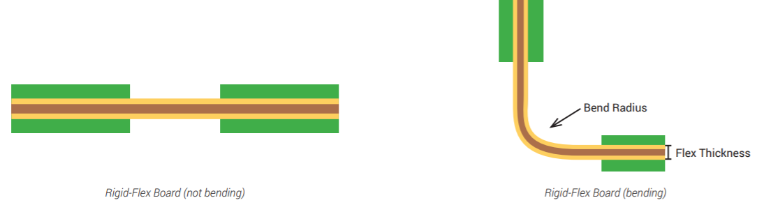
Rigid-flex PCBs combine rigid and flexible sections to meet space constraints in electronics. Via design plays a key role in rigid-flex PCB via design for reliable signal paths and structural integrity. Poor via placement leads to failures like cracks during flexing or high resistance in signals. Industry standards such as IPC-6013 and IPC-2223 guide via requirements for performance classes. Optimizing vias improves electrical continuity and mechanical reliability. Engineers must balance density with durability in these hybrid boards.
Understanding PCB Via Types in Rigid-Flex Designs
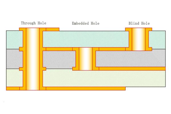
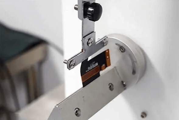
Rigid-flex PCBs use various PCB via types to connect layers across rigid and flex regions. Through-hole vias span the entire board thickness for simple interconnections. Blind vias link an outer layer to an inner layer without full penetration. Buried vias connect only internal layers and remain hidden from surfaces. Each type suits specific needs in rigid-flex PCB via design. Through vias work well in rigid areas but risk stress in flex zones.
Blind and buried vias save space and reduce weight in high-density layouts. They allow tighter routing by avoiding outer layer holes. In flex sections, these vias minimize exposure to bending forces. Engineers select blind vias for outer-to-inner links in rigid parts. Buried vias suit multilayer rigid cores for signal integrity. Proper choice prevents delamination at rigid-flex transitions.
Why Via Design Matters in Rigid-Flex PCBs
Vias ensure current flow and heat transfer in rigid-flex assemblies. In flex areas, vias face repeated bending that causes fatigue. Rigid sections demand vias for power distribution without impedance issues. Mechanical stress at transitions amplifies via failure risks. Electrical performance suffers from via inductance in high-speed signals. Optimized rigid-flex PCB via design extends board life and reliability.
Poor via placement increases trace lengths and signal loss. Flexing induces shear on via barrels leading to opens. Thermal expansion mismatches crack vias over cycles. Standards like IPC-2223 define via annular ring sizes for strength. Engineers prioritize via location to avoid bend zones. This approach enhances overall board performance.
Technical Principles of Via Stitching and Grounding
Via stitching uses multiple vias to tie planes for low impedance paths. It distributes current evenly across ground or power planes. In rigid-flex PCBs, stitching reduces voltage drops in high-current areas. Vias form a fence-like pattern around components or signals. This technique lowers inductance for better EMI control. Stitching spacing depends on frequency and current needs.
Ground via stitching connects flex ground layers to rigid planes. It maintains shield integrity during flexure. Patterns like grids or arrays optimize coverage without excess density. Engineers calculate stitch density based on skin effect at operating frequencies. Over-stitching wastes space and raises costs. Balanced use improves electrical performance.
Thermal Vias in PCB Design for Heat Management
Thermal vias PCB designs channel heat from components to inner planes. Arrays of small vias under hotspots spread thermal loads. Copper plating fills vias for better conduction. In rigid-flex, thermal vias stay in rigid sections to avoid flex cracks. They pair with thick copper planes for dissipation. Via diameter and pitch control airflow resistance.
Blind thermal vias limit exposure in multilayer stacks. They connect heat sources to buried planes efficiently. Pitch of 0.5 mm to 1 mm suits most power devices. Filled vias prevent solder wicking during assembly. Engineers model thermal resistance with via count and size. This prevents hotspots in dense rigid-flex layouts.
Mechanical Considerations in Rigid-Flex Via Optimization
Rigid-flex PCBs endure dynamic flexing that stresses vias. Vias near bend lines crack from cyclic strain. Rigid cores handle through vias better than flex layers. Transition zones need staggered vias to distribute loads. Aspect ratios under 8:1 ensure plating uniformity per IPC-6013. Engineers offset vias from flex edges by at least 1 mm.
Buried and blind vias reduce surface stress in flex regions. They limit plating exposure to mechanical wear. Stackup planning aligns vias with rigid reinforcements. Simulation tools predict strain at via sites. Material CTE matching aids via reliability. These steps boost mechanical endurance.
Best Practices for Rigid-Flex PCB Via Design
Start with stackup review for via feasibility across regions. Use blind and buried vias in high-density rigid areas. Limit through vias to rigid sections only. Maintain 0.15 mm minimum annular ring for strength. Group thermal vias PCB under power components with 10-20 per mm2 arrays. Verify aspect ratios below 10:1 for blind types.
Implement via stitching at 2-5 mm intervals for planes. Tent unused vias to protect from solder. Fill high-current vias with conductive epoxy. Prototype tests check via continuity after flex cycles. Collaborate on DFM for laser drilling precision. These practices ensure robust rigid-flex PCB via design.
For via stitching, align patterns to trace returns. Thermal vias need epoxy fill for reliability in reflow. Blind vias require sequential lamination control. Document via maps in fab drawings. Simulate signal integrity pre-layout. Follow these for optimal performance.
Troubleshooting Common Via Issues in Rigid-Flex PCBs
Cracked vias signal excessive bend radius or poor placement. Inspect with cross-sectioning after prototypes. Delamination around vias points to plating voids. Use X-ray for buried via checks. High resistance indicates under-plating; measure with TDR. Adjust drill sizes for better copper adhesion.
Thermal vias clogging reduces heat flow; ensure fill processes. Stitching failures show from EMI spikes; add more vias. Blind via opens stem from laser alignment errors. Rework with microvia fills if needed. Log failures to refine designs. Systematic checks maintain quality.
Conclusion
Rigid-flex PCB via design demands careful selection of PCB via types like blind and buried vias. Via stitching and thermal vias PCB enhance electrical flow and cooling. Mechanical rules protect against flex fatigue. Adhering to IPC standards ensures compliance. Engineers gain reliable boards through structured optimization. Apply these principles for superior performance.
FAQs
Q1: What are blind and buried vias in rigid-flex PCB via design?
A1: Blind vias connect outer to inner layers without full board penetration. Buried vias link only internal layers for dense routing. In rigid-flex, they avoid stress in flex areas. Use them to save space and improve signal integrity. Proper aspect ratios under 8:1 aid plating. They suit high-reliability applications.
Q2: How does via stitching improve performance in rigid-flex PCBs?
A2: Via stitching ties planes with multiple vias for low-impedance paths. It distributes currents and reduces inductance. Place grids around high-speed signals. In rigid-flex, it maintains ground continuity across bends. Optimal spacing is 2-5 mm based on needs. This boosts EMI control and power delivery.
Q3: When should thermal vias PCB be used in rigid-flex designs?
A3: Thermal vias PCB dissipate heat from components to planes. Array them under power devices in rigid sections. Use 0.3 mm diameter with 1 mm pitch. Fill with copper for best conduction. Avoid in flex zones to prevent cracks. They lower junction temperatures effectively.
Q4: What challenges arise with PCB via types in rigid-flex transitions?
A4: Through vias risk cracks at rigid-flex borders from strain. Blind and buried vias mitigate this issue. Offset them from bend lines by 1 mm. Control stackup for alignment. Test prototypes for continuity post-flex. Optimization ensures durability.
References
IPC-6013D — Qualification and Performance Specification for Flexible and Rigid-Flex Printed Boards. IPC, 2017
IPC-2223C — Sectional Design Standard for Flexible/Rigid-Flexible Printed Boards. IPC, 2017