Introduction
High-density printed circuit boards (PCBs) are the backbone of modern electronics, enabling compact designs with complex functionality. However, as signal speeds increase and board layouts become denser, managing impedance discontinuity poses significant challenges. These discontinuities can disrupt signal integrity, leading to reflections, crosstalk, and performance degradation in high-speed applications. For electrical engineers, understanding and mitigating these issues through controlled impedance routing and design for manufacturability (DFM) practices is critical. This article explores the root causes of impedance discontinuity, the importance of trace impedance control, and actionable strategies for optimizing high-density PCB designs. By focusing on practical solutions and adhering to industry standards, engineers can ensure reliable performance in demanding applications.
What Is Impedance Discontinuity and Why It Matters
Impedance discontinuity occurs when there is a mismatch in the characteristic impedance along a signal path on a PCB. This mismatch can arise from changes in trace geometry, layer transitions, or material variations, causing signal reflections that distort data transmission. In high-speed designs, where signals operate at gigahertz frequencies, even minor discontinuities can lead to significant errors, affecting system reliability.
The importance of addressing impedance discontinuity cannot be overstated. Signal reflections resulting from mismatches can cause timing issues, increased noise, and electromagnetic interference (EMI). For applications like telecommunications, automotive electronics, and data centers, these problems can compromise functionality. Controlled impedance routing ensures that the trace impedance remains consistent, minimizing reflections and maintaining signal integrity. By integrating DFM principles, engineers can design boards that are not only high-performing but also manufacturable with precision.
Technical Principles of Impedance Discontinuity
Impedance in PCB design refers to the opposition a signal encounters as it travels along a trace. The characteristic impedance of a trace depends on factors such as its width, thickness, spacing, and the dielectric properties of the surrounding materials. When this impedance changes abruptly due to design or manufacturing variations, a discontinuity occurs.
Signal reflections are a primary consequence of impedance discontinuity. When a signal encounters a mismatch, part of the energy reflects back toward the source, interfering with the original signal. This can lead to overshoot, undershoot, or ringing, all of which degrade performance. The severity of reflections depends on the magnitude of the mismatch and the signal frequency. Higher frequencies are more susceptible due to shorter wavelengths, making high-speed designs particularly vulnerable.
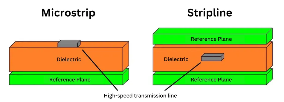
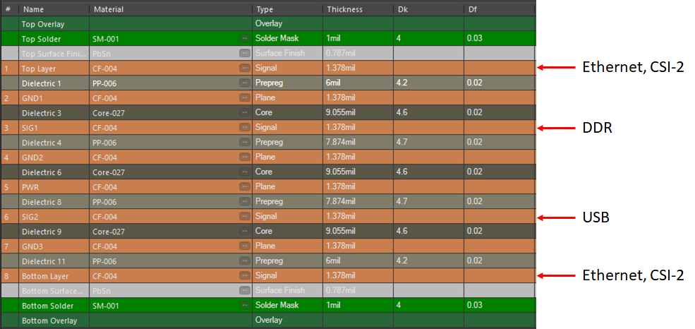
Another key consideration is the choice between microstrip and stripline configurations. Microstrip traces, located on the outer layers of a PCB, are exposed to air on one side, resulting in higher impedance for a given width compared to stripline. Stripline traces, embedded between two ground planes, offer better shielding and lower impedance but are more complex to manufacture. Understanding the differences between microstrip vs stripline is essential for selecting the appropriate structure to minimize discontinuities.
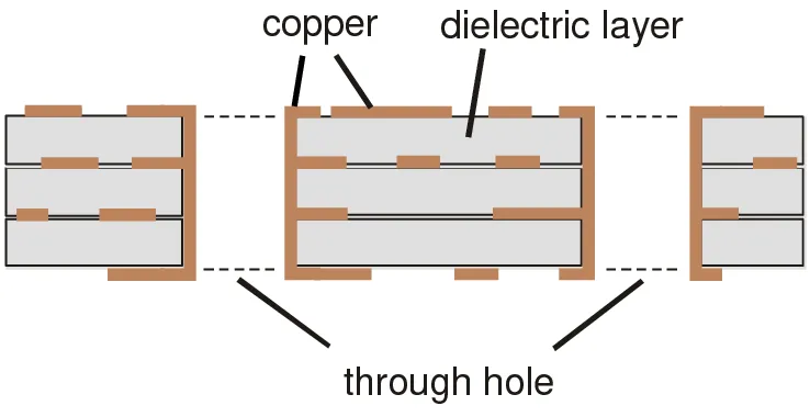
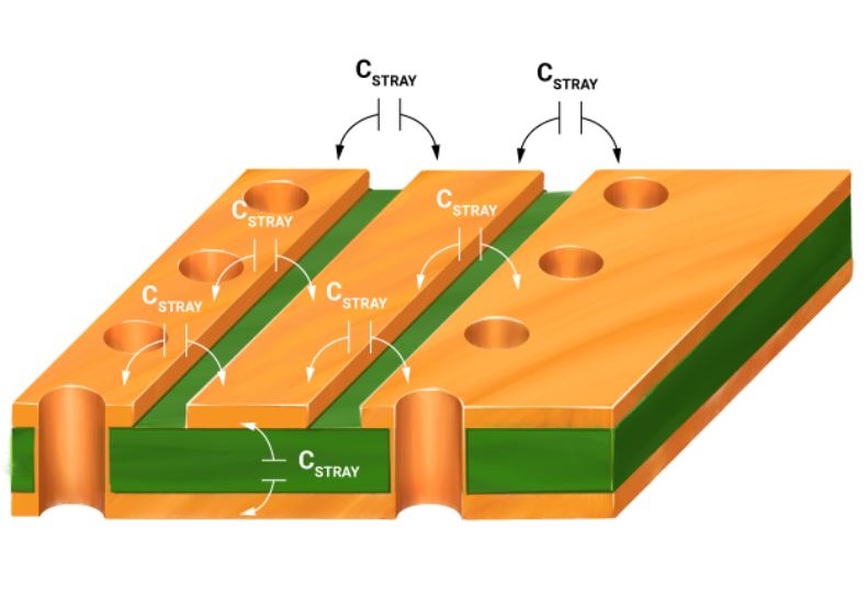
Layer transitions, connectors, and vias also contribute to impedance mismatches. For instance, a via connecting a trace from one layer to another introduces inductance and capacitance, altering the impedance profile. Similarly, changes in trace width or spacing near components can create discontinuities. Recognizing these mechanisms allows engineers to address potential issues during the design phase.
Causes of Impedance Discontinuity in High-Density PCBs
High-density PCBs, with their compact layouts and numerous components, are particularly prone to impedance issues. Several factors contribute to discontinuities in these designs:
- Trace Geometry Variations: Inconsistent trace widths or thicknesses due to manufacturing tolerances can alter impedance. Narrower traces increase impedance, while wider traces reduce it.
- Layer Transitions: Signals moving between layers through vias experience impedance changes due to differences in dielectric constants or via parasitics.
- Material Inhomogeneity: Variations in the dielectric constant of PCB substrates can affect signal propagation, especially in high-frequency designs.
- Component Pads and Connectors: Large pads or poorly matched connectors introduce capacitance, disrupting the impedance profile.
- Routing Near Edges or Splits: Traces routed near board edges or over splits in ground planes can experience impedance shifts due to altered return paths.
Addressing these causes requires a combination of precise design practices and an understanding of manufacturing limitations. Standards such as IPC-6012E provide guidelines for ensuring consistent trace geometries and material properties during fabrication.
Practical Solutions for Controlled Impedance Routing
Achieving controlled impedance routing in high-density PCBs demands a systematic approach. Below are actionable strategies that engineers can implement to minimize impedance discontinuity and ensure signal integrity.
Define Target Impedance Early
Establishing the target trace impedance at the outset is crucial. This value depends on the signal standard, such as 50 ohms for many high-speed applications. Use impedance calculators or simulation tools to determine the required trace width, spacing, and dielectric thickness based on the chosen substrate material.
Optimize Trace Geometry
Maintain uniform trace widths and thicknesses along the signal path. Avoid abrupt changes in geometry, especially near vias or component pads. If width adjustments are necessary, implement gradual tapers to minimize reflections. Adhering to tolerances specified in IPC-A-600K ensures manufacturability and consistency.
Select Appropriate Layer Stackup
Choose between microstrip and stripline configurations based on design requirements. Microstrip is simpler to fabricate and inspect but offers less EMI protection. Stripline provides better shielding but requires precise control over dielectric thickness. Ensure the stackup design aligns with the target impedance by collaborating with fabrication teams early.
Minimize Via Effects
Vias are unavoidable in high-density designs, but their impact on impedance can be reduced. Use back-drilling to remove unused via stubs, which can cause reflections. Additionally, place ground vias near signal vias to provide a low-impedance return path. This practice helps maintain signal integrity across layer transitions.
Ensure Continuous Return Paths
A solid and continuous ground plane beneath signal traces prevents impedance discontinuity. Avoid routing high-speed signals over splits or gaps in the ground plane, as this disrupts the return path and increases reflections. For multilayer boards, dedicate entire layers to ground to enhance shielding.
Account for Manufacturing Tolerances
DFM principles are essential for controlled impedance routing. Work within the fabrication tolerances outlined in standards like IPC-6012E to ensure that trace dimensions and material properties remain consistent. Specify controlled impedance requirements clearly in design documentation to guide manufacturers.
Best Practices for DFM in High-Density PCB Design
Design for manufacturability plays a pivotal role in overcoming impedance challenges. By aligning design choices with fabrication capabilities, engineers can achieve reliable controlled impedance routing. Consider the following best practices:
- Collaborate with Fabricators: Engage with manufacturing teams during the design phase to understand their process capabilities and limitations. This ensures that impedance specifications are achievable.
- Specify Material Properties: Select PCB substrates with consistent dielectric constants and low loss tangents for high-frequency signals. Clearly document these requirements to avoid variations during production.
- Test and Validate Designs: Use simulation tools to model impedance profiles and identify potential discontinuities before fabrication. Post-manufacturing testing, guided by IPC-A-600K, can verify impedance values.
- Standardize Routing Rules: Establish design rules for trace spacing, width, and via placement to maintain consistency across the board. Automate these rules in design software to reduce errors.
Implementing these practices not only mitigates impedance discontinuity but also streamlines the transition from design to production, reducing costly iterations.
Insight: Balancing Performance and Manufacturability
For electrical engineers, striking a balance between performance and manufacturability is a constant challenge in high-density PCB design. While tight impedance control is necessary for signal integrity, overly stringent specifications can complicate fabrication and increase costs. A practical approach involves prioritizing critical signal paths for controlled impedance routing while allowing more flexibility for non-critical traces. Additionally, iterative feedback from manufacturing teams can refine designs to align with production realities. By focusing on DFM principles and adhering to standards like IPC-6012E, engineers can create boards that perform reliably without exceeding fabrication capabilities.
Conclusion
Impedance discontinuity poses a significant hurdle in high-density PCB design, particularly for high-speed applications where signal integrity is paramount. By understanding the causes of discontinuities, such as trace geometry variations and layer transitions, engineers can implement controlled impedance routing to minimize signal reflections. Practical solutions, including optimized trace design, careful stackup planning, and DFM best practices, ensure that designs are both high-performing and manufacturable. Adhering to industry standards provides a foundation for consistency and reliability. Through meticulous planning and collaboration, electrical engineers can overcome impedance challenges and deliver robust PCB solutions for modern electronics.
FAQs
Q1: What causes impedance discontinuity in high-density PCBs?
A1: Impedance discontinuity arises from mismatches in trace impedance due to variations in trace width, layer transitions, or material properties. Vias, connectors, and routing over ground plane splits can also disrupt signal paths. These issues lead to signal reflections, impacting performance in high-speed designs. Addressing them requires uniform geometry and continuous return paths.
Q2: How does controlled impedance routing improve signal integrity?
A2: Controlled impedance routing maintains a consistent trace impedance along signal paths, reducing reflections and crosstalk. By matching the impedance to the system requirements, it ensures clean signal transmission. This is vital for high-frequency applications where timing and noise margins are tight, enhancing overall reliability.
Q3: What are the differences between microstrip vs stripline in impedance control?
A3: Microstrip traces, on outer layers, have higher impedance and less shielding, making them simpler to fabricate but prone to EMI. Stripline, embedded between ground planes, offers lower impedance and better noise protection but is harder to manufacture. Choosing between them depends on design needs and impedance targets.
Q4: How can DFM practices help with trace impedance in PCB design?
A4: DFM practices align design with manufacturing capabilities, ensuring trace impedance specifications are achievable. Collaboration with fabricators, specifying material properties, and adhering to tolerances prevent variations. This approach minimizes discontinuities, reduces production errors, and ensures consistent performance in high-density PCB layouts.
References
IPC-6012E — Qualification and Performance Specification for Rigid Printed Boards. IPC, 2020.
IPC-A-600K — Acceptability of Printed Boards. IPC, 2020.