Introduction
High-density metal core printed circuit boards (MCPCBs) play a critical role in modern electronics, especially in applications requiring efficient heat dissipation and compact layouts. These boards, often used in power electronics, LED lighting, and automotive systems, face unique manufacturing challenges due to their complex designs and thermal management needs. Electrical engineers must navigate issues in fabrication, trace routing, circuit design, and cost reduction to ensure reliability and performance. This article explores the core obstacles in producing high-density MCPCBs and offers practical solutions grounded in industry standards. By addressing these challenges, engineers can optimize designs for both functionality and manufacturability, ensuring that projects meet stringent quality and budget requirements.
What Are High-Density MCPCBs and Why Do They Matter?
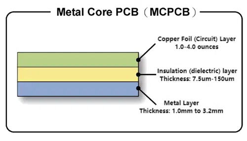
MCPCBs differ from standard PCBs due to their metal substrate, typically aluminum or copper, which enhances thermal conductivity. High-density designs incorporate tightly packed components and intricate trace patterns, often on multiple layers, to support advanced circuitry in limited space. These multilayer circuit boards are essential in industries where heat management is paramount, as they prevent overheating of sensitive components. Their relevance continues to grow with the rise of compact, high-power devices. However, the combination of dense layouts and metal cores introduces complexities in fabrication and circuit design. Overcoming these hurdles ensures that MCPCBs meet performance expectations while maintaining cost efficiency, a key concern for engineers balancing innovation with practical constraints.
Technical Challenges in High-Density MCPCB Manufacturing
Fabrication Complexities
Fabricating high-density MCPCBs involves precise control over material selection and layer bonding. The metal core, while excellent for heat dissipation, complicates drilling and cutting processes due to its hardness. Misalignment during lamination can lead to delamination or poor dielectric integrity, risking electrical failures. Additionally, achieving uniform thickness across the board is difficult, as variations can impact thermal performance. Standards such as IPC-6012E provide guidelines for rigid board performance, emphasizing the need for consistent manufacturing processes to avoid defects. Engineers must also consider the thermal expansion mismatch between the metal core and dielectric layers, which can cause stress during production or operation.
Trace Routing Difficulties
Trace routing in high-density MCPCBs is a significant challenge due to limited space and the need for precise signal integrity. Narrow traces and small vias are necessary to accommodate numerous connections, but this increases the risk of crosstalk and signal loss. The metal core can also interfere with electromagnetic performance if not properly insulated. Routing must account for thermal paths, ensuring heat dissipation does not compromise electrical performance. Adhering to standards like IPC-A-600K for acceptability criteria helps maintain trace quality, but engineers must balance density with manufacturability to prevent issues during etching or plating stages.
Circuit Design Constraints
Circuit design for high-density MCPCBs requires careful planning to integrate complex functionality within confined areas. Component placement must optimize both electrical connections and thermal management, often necessitating advanced simulation tools to predict heat flow. Power and ground planes need strategic positioning to minimize noise, while vias must be placed to avoid thermal hotspots. The challenge intensifies with multilayer designs, where interlayer alignment is critical. Following guidelines from IPC-6012E ensures that performance specifications are met, but designers must also anticipate fabrication limitations to avoid costly redesigns.
Cost Reduction Pressures
Cost reduction remains a persistent concern in high-density MCPCB production. The use of metal cores and specialized dielectric materials increases material expenses compared to standard PCBs. Fabrication processes, such as precision drilling and advanced plating, further elevate costs. Additionally, high-density designs often require tighter tolerances, leading to higher rejection rates if quality standards are not met. Engineers face the task of optimizing designs to minimize waste and reduce manufacturing complexity without sacrificing reliability. Balancing these factors is essential to deliver cost-effective solutions that meet project budgets.
Suggested Reading: The Cost Breakdown of Metal Core PCBs: What Drives the Price?
Practical Solutions for High-Density MCPCB Challenges
Streamlining Fabrication Processes
To address fabrication challenges, engineers should prioritize material compatibility and process control. Selecting dielectric materials with thermal expansion coefficients close to the metal core reduces stress during manufacturing. Implementing strict quality checks, aligned with IPC-A-600K, during lamination and drilling stages helps detect defects early. Automated equipment for precise alignment can minimize human error, ensuring consistent board thickness. Additionally, collaborating with manufacturing teams to define achievable tolerances prevents over-specification, which can drive up costs unnecessarily. Regular audits of production workflows, based on ISO 9001:2015 principles, further enhance reliability.
Optimizing Trace Routing Techniques
Effective trace routing starts with thorough planning during the design phase. Utilizing wider traces where possible reduces resistance and improves signal integrity, even in dense layouts. Differential pair routing can minimize crosstalk, while strategic via placement avoids interference with thermal paths. Simulation software helps identify potential issues before fabrication, allowing adjustments to trace patterns. Compliance with IPC-6012E ensures that trace dimensions meet performance criteria, reducing the likelihood of manufacturing errors. Engineers should also consider layer stacking to segregate high-speed signals from power lines, enhancing overall board performance.
Enhancing Circuit Design Strategies
Circuit design improvements for high-density MCPCBs focus on thermal and electrical optimization. Placing heat-generating components near the metal core maximizes heat dissipation, while spacing sensitive elements away from hotspots protects performance. Multilayer designs should incorporate thermal vias to transfer heat efficiently across layers. Power plane distribution must be uniform to avoid voltage drops, and ground planes should cover sufficient area to reduce noise. Adhering to standards like JEDEC J-STD-020E for moisture sensitivity during design prevents reliability issues post-fabrication. Iterative testing and simulation refine layouts for both functionality and manufacturability.
Achieving Cost Reduction Goals
Cost reduction in high-density MCPCB production requires a multi-faceted approach. Simplifying designs by reducing layer counts where feasible lowers material and processing expenses. Standardizing component sizes minimizes the need for custom fabrication steps, aligning with efficient manufacturing practices. Engineers can also explore alternative materials with comparable thermal properties but lower costs, provided they meet industry standards like IPC-6012E. Bulk purchasing of raw materials and optimizing board panelization reduces waste during production. Finally, early collaboration between design and manufacturing teams identifies cost-saving opportunities without compromising quality.
Troubleshooting Common Issues in High-Density MCPCB Designs
High-density MCPCBs often encounter specific issues that require targeted troubleshooting. Warpage, for instance, can occur due to uneven thermal expansion during fabrication. Testing for warpage, as outlined in IPC-A-600K, involves precise measurement to ensure flatness within acceptable limits. If warpage exceeds tolerances, adjusting material choices or lamination parameters may resolve the issue. Another common problem is poor trace adhesion, often caused by inadequate surface preparation. Enhancing cleaning processes before plating improves adhesion and prevents delamination. Electrical shorts due to tight trace spacing can be mitigated by revising routing patterns and increasing clearance where possible. Documenting these solutions ensures consistent application across future projects.
Conclusion
High-density MCPCB designs present unique manufacturing challenges in fabrication, trace routing, circuit design, and cost reduction. By understanding the technical complexities, such as material compatibility and thermal management, engineers can implement practical solutions to enhance reliability and performance. Streamlining production processes, optimizing layouts, and adhering to recognized standards like IPC-6012E and IPC-A-600K are essential steps in overcoming these obstacles. Cost reduction, while challenging, is achievable through design simplification and strategic collaboration. With these approaches, electrical engineers can successfully navigate the intricacies of high-density MCPCB manufacturing, delivering innovative solutions for demanding applications.
FAQs
Q1: How does fabrication impact the reliability of high-density MCPCBs?
A1: Fabrication significantly affects high-density MCPCB reliability due to the complexity of bonding metal cores with dielectric layers. Misalignment or poor lamination can lead to delamination, risking electrical failures. Following standards like IPC-6012E ensures consistent quality during drilling and cutting. Precise control over material selection and process parameters minimizes defects, enhancing long-term performance in thermal and electrical applications.
Q2: What are key considerations for trace routing in dense MCPCB layouts?
A2: Trace routing in dense MCPCB layouts requires balancing signal integrity with spatial constraints. Narrow traces increase crosstalk risk, so wider traces or differential pairs are preferred where space allows. Strategic via placement avoids thermal interference. Compliance with IPC-A-600K helps maintain trace quality, while simulation tools identify issues early, ensuring manufacturability without compromising electrical performance.
Q3: How can circuit design optimize thermal management in MCPCBs?
A3: Circuit design optimizes thermal management by placing heat-generating components near the metal core for efficient dissipation. Thermal vias transfer heat across layers, and spacing sensitive parts from hotspots protects functionality. Uniform power plane distribution reduces voltage drops. Adhering to JEDEC J-STD-020E for moisture sensitivity during design prevents thermal stress issues, ensuring reliable operation in high-density setups.
Q4: What strategies support cost reduction in high-density MCPCB production?
A4: Cost reduction in high-density MCPCB production involves simplifying designs by minimizing layer counts and standardizing components to lower fabrication expenses. Exploring cost-effective materials with adequate thermal properties, per IPC-6012E, helps manage budgets. Efficient panelization reduces waste, and early design-manufacturing collaboration identifies savings. These steps maintain quality while addressing financial constraints effectively.
References
IPC-6012E - Qualification and Performance Specification for Rigid Printed Boards. IPC, 2020.
IPC-A-600K - Acceptability of Printed Boards. IPC, 2020.
JEDEC J-STD-020E - Moisture/Reflow Sensitivity Classification. JEDEC, 2014.
ISO 9001:2015 - Quality Management Systems. ISO, 2015.


