Introduction
Printed circuit board (PCB) manufacturing involves complex processes where even minor variations can lead to significant defects, impacting product reliability and yield. Electric engineers often encounter PCB manufacturing defects such as delamination, warpage, and plating voids during production runs, which can escalate costs and delay timelines. Addressing these PCB production issues requires a deep understanding of material interactions, process controls, and inspection methods aligned with industry standards. This guide serves as a PCB troubleshooting guide, offering factory-driven insights into common PCB errors and practical strategies for preventing PCB defects. By focusing on root causes and proven solutions, engineers can optimize fabrication outcomes and ensure high-quality boards. Ultimately, proactive measures in design and manufacturing minimize rework and enhance overall performance.
Why PCB Manufacturing Defects Matter in Production
PCB manufacturing defects compromise electrical integrity, mechanical stability, and long-term reliability, making them critical concerns for electric engineers in high-stakes applications. These issues arise during lamination, drilling, plating, and etching, potentially leading to field failures if undetected. For instance, undetected voids in plating can cause intermittent connections under thermal stress, while warpage affects assembly precision. Industry standards like IPC-6012 define qualification criteria to mitigate such risks, emphasizing performance specifications for rigid boards. Preventing PCB defects not only boosts yield rates but also aligns with quality management systems such as ISO 9001, fostering consistent production. Engineers must prioritize these challenges to meet stringent requirements in sectors demanding robust electronics.
Common Causes of PCB Manufacturing Defects
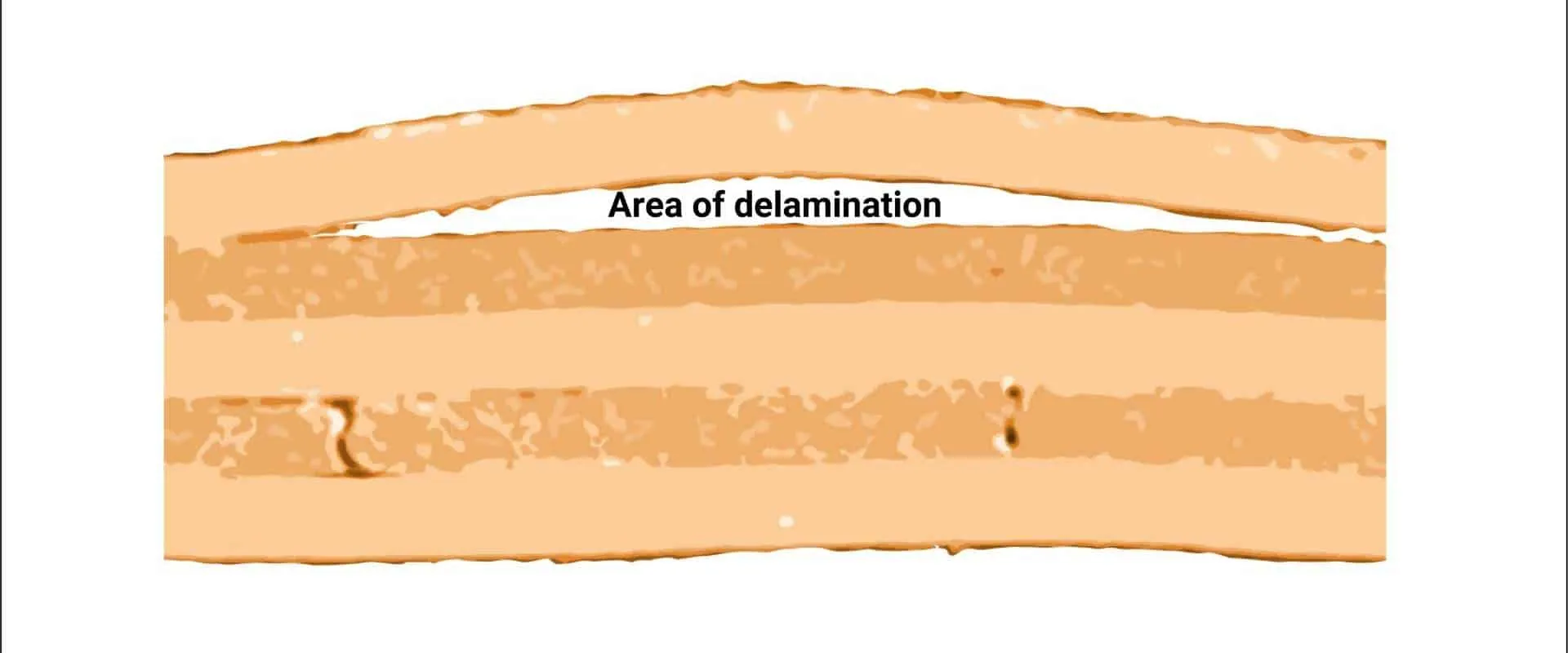
Delamination: Mechanisms and Triggers
Delamination occurs when layers separate due to poor adhesion between copper foil and prepreg, often triggered by moisture absorption during storage or inadequate lamination pressure. Excessive heat in multilayer presses exacerbates this by causing resin degradation or voids that expand under thermal cycling. Contamination from handling or improper surface preparation further weakens bonds, leading to blistering visible post-etching. Factory processes must control bake-out cycles to desorb moisture, as per guidelines in IPC-A-600 for acceptability criteria. Engineers observe this defect more in high-layer-count boards where CTE mismatches between materials amplify stresses. Understanding these mechanisms enables targeted interventions early in the production flow.
Warpage and Bow: Thermal and Material Factors
Warpage manifests as dimensional distortion, primarily from asymmetric copper distribution or mismatched coefficients of thermal expansion (CTE) in stackups. During lamination, uneven cooling rates cause residual stresses that bow the board beyond allowable limits, complicating automated assembly. Thinner boards or those with large copper planes on one side are particularly susceptible, as heat dissipation varies across layers. IPC-6012 specifies maximum bow and twist tolerances based on board size and thickness to ensure flatness for soldering. Production data shows warpage intensifying post-plating due to electroplating stresses. Electric engineers can model these effects using stackup simulations to predict and adjust for balanced layouts.
Plating Voids and Blowholing: Process-Related Issues
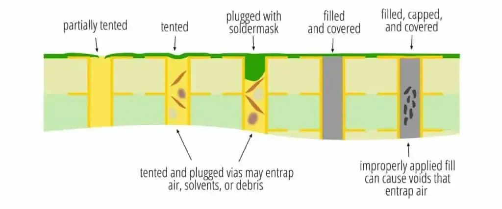
Plating voids, including blowholing, stem from trapped gases or contaminants in drilled holes that escape during electroplating, creating barrel wall discontinuities. Inadequate desmear processes leave resin residue, which outgases under plating current, pitting the copper deposit. High aspect ratio vias compound this by limiting electrolyte flow and renewal. J-STD-020 outlines moisture sensitivity handling to prevent such defects from absorbed water vaporizing in reflow-like conditions during fab. Factories mitigate this through plasma etching or optimized chemical desmear, ensuring uniform plating thickness. These PCB production issues demand rigorous hole preparation to maintain via reliability.
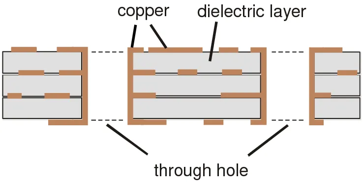
Via and Hole Wall Defects: Drilling and Plating Challenges
Drill breakout, smear, and dogboning result from mechanical drilling inaccuracies or excessive heat, where the drill bit wanders or chisels the entry/exit, reducing annular rings. Plating then fails to cover breakout areas adequately, per IPC-A-600 visual standards. High-speed drilling without proper entry materials generates burrs that interfere with plating adhesion. Voids in electroless copper seed layers propagate to electrolytic plating, weakening barrel integrity. Engineers address this by selecting controlled-depth drills and entry boards, alongside post-drill inspections. Consistent tooling management prevents these common PCB errors across production batches.
Practical Solutions for Solving PCB Problems
Best Practices to Prevent Delamination
To combat delamination, implement strict material storage protocols with humidity-controlled environments below 50% RH, followed by bake-out at specified temperatures prior to lamination. Optimize press cycles with ramped pressure and temperature profiles to achieve full resin flow without scorching. Surface activation via plasma or chemical treatments enhances adhesion, verifiable through peel strength tests. IPC-6012 performance specs guide qualification of laminates for delamination resistance under thermal shock. Factory audits of prepreg quality and copper foil roughness ensure consistency. Regular cross-section analysis post-lamination catches incipient issues early.
Strategies for Minimizing Warpage
Balancing copper weight across layers through symmetric stackups and fill adjustments counters warpage effectively. Use low-CTE core materials and constrain designs with fixtures during cooling. Post-lamination baking relieves stresses, while routing panels with fiducials aids precise measurement against IPC-6012 tolerances. Simulate warpage using finite element analysis incorporating material datasheets for accurate predictions. Production trials with varied cure cycles refine processes for flatness. These steps form a comprehensive PCB troubleshooting guide for maintaining dimensional stability.
Eliminating Plating Voids and Blowholing
Enhance desmear efficacy with permanganate or plasma processes, followed by residue-free rinses to eliminate outgassing sources. Control plating bath chemistry, including brighteners and current density, for void-free deposits in high-aspect holes. Pre-plating vacuum degassing removes entrapped air from vias. Adherence to J-STD-020 for handling prevents moisture-induced defects. Microsection sampling at key process points validates improvements. Engineers benefit from statistical process control to track plating uniformity across panels.
Optimizing Via Quality and Hole Preparation
Employ laser or controlled-depth mechanical drilling for precise hole geometries, minimizing wander and smear. Backup and entry materials capture chips, reducing burrs per IPC-A-600 criteria. Post-drill plasma cleaning ensures clean walls before plating. Aspect ratios below 10:1 facilitate plating, with pulse plating for deep vias. Inline electrical testing detects opens early. These factory-driven practices resolve via-related PCB manufacturing defects systematically.
Troubleshooting Insights for Production Issues
When diagnosing batches with recurring defects, start with process mapping to isolate variables like drill speed or bath agitation. Cross-sections and SEM analysis reveal root causes, such as inadequate desmear for voids. Correlate defect maps with panel locations to identify equipment hotspots. Implement SPC charts tracking key metrics like plating thickness and bow. Collaborate with material suppliers for CTE-matched laminates. This structured approach, informed by IPC-9121 troubleshooting guidelines, accelerates yield recovery.
Conclusion
Overcoming PCB manufacturing challenges demands vigilance across design, materials, and processes to tackle defects like delamination, warpage, and plating voids. By applying standard-aligned best practices, electric engineers can prevent PCB defects, enhance production yields, and deliver reliable boards. Key strategies include balanced stackups, rigorous desmear, and precise drilling, all verifiable against IPC and J-STD criteria. This PCB troubleshooting guide equips teams to solve PCB problems proactively, reducing costs and downtime. Consistent adherence to quality systems ensures long-term success in fabrication. Prioritize these insights for superior outcomes in every run.
FAQs
Q1: What are the most common PCB manufacturing defects and how can engineers prevent them?
A1: Common PCB manufacturing defects include delamination from moisture, warpage due to CTE mismatch, and plating voids from poor desmear. Prevention involves humidity-controlled storage, symmetric stackups, and plasma cleaning before plating. Adhering to IPC-6012 tolerances during qualification verifies effectiveness. Regular process audits maintain consistency, minimizing rejects in production.
Q2: How does IPC-A-600 help in solving PCB production issues?
A2: IPC-A-600 provides visual acceptability criteria for defects like annular ring reductions and measling, guiding inspections post-fabrication. Engineers use it to classify issues by class levels, prioritizing fixes for Class 3 boards. It standardizes defect calls across teams, accelerating troubleshooting. This ensures production aligns with performance specs.
Q3: What causes plating voids in PCBs and what is the best prevention strategy?
A3: Plating voids arise from outgassing drill residues or air entrapment in high-aspect vias during electroplating. Optimal prevention uses chemical or plasma desmear, vacuum degassing, and controlled current densities. J-STD-020 handling avoids moisture contributions. Microsection verification confirms void-free barrels.
Q4: Why is warpage a critical PCB production issue and how to measure it?
A4: Warpage hinders assembly by misaligning pads, stemming from uneven copper or cooling stresses. Measure using dial gauges or laser systems against IPC-6012 limits, typically 0.75% for panels. Prevention via balanced designs and stress-relief bakes resolves it effectively.
References
IPC-6012E — Qualification and Performance Specification for Rigid Printed Boards. IPC, 2017
IPC-A-600K — Acceptability of Printed Boards. IPC, 2020
J-STD-020E — Moisture/Reflow Sensitivity Classification. JEDEC, 2014
IPC-9121 — Troubleshooting for Printed Board Fabrication Processes. IPC, 2020