Introduction
Panel design for manufacturing plays a pivotal role in the production of printed circuit boards, ensuring efficiency, quality, and cost effectiveness. For electrical engineers, understanding the art of DFM, or Design for Manufacturing, is essential to streamline processes and achieve optimal results. This approach focuses on improving quality while reducing cost by integrating manufacturing considerations early in the design phase. By prioritizing DFM principles, engineers can minimize production errors, reduce material waste, and enhance product reliability. This article provides a detailed exploration of panel design strategies, technical principles, and best practices tailored for professionals in the field. From panelization techniques to compliance with industry standards, the content aims to equip engineers with actionable insights for successful manufacturing outcomes.
What Is Panel Design for Manufacturing and Why It Matters
Panel design for manufacturing refers to the process of arranging multiple printed circuit board layouts into a single panel for efficient production. This step is critical in mass production as it maximizes material usage and simplifies handling during fabrication and assembly. By grouping individual boards into a panel, manufacturers can process several units simultaneously, reducing setup times and costs. For electrical engineers, mastering the art of DFM in panel design directly impacts the scalability of production. A well designed panel ensures uniform processing conditions, which is vital for improving quality while reducing cost. Poor panel design, on the other hand, can lead to issues like uneven etching, mechanical stress, or assembly errors, ultimately increasing expenses and delays. Thus, strategic panelization is not just a manufacturing step but a cornerstone of reliable and economical production.
Technical Principles of Panel Design for Manufacturing
Panel design involves several technical considerations to ensure manufacturability and quality. The primary goal is to balance the number of boards per panel with the constraints of fabrication equipment and material properties. Key principles include maintaining consistent spacing, ensuring structural integrity, and adhering to industry standards for tolerances.
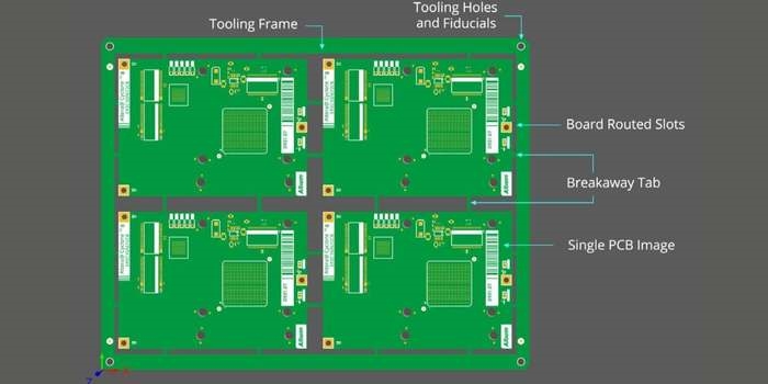
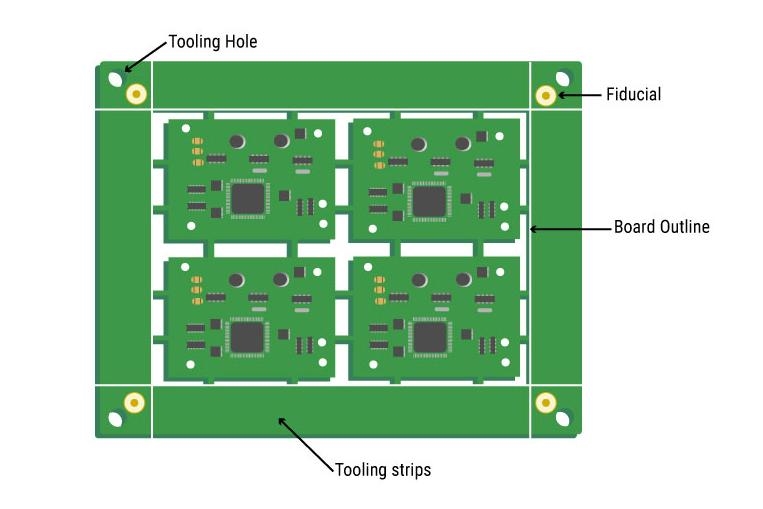
One fundamental aspect is the selection of panel size, which must align with the capabilities of fabrication and assembly machinery. Standard panel sizes often follow guidelines outlined in documents like IPC-6012E, which specifies performance requirements for rigid boards. Spacing between individual boards, known as breakaway tabs or mouse bites, must be carefully calculated to allow easy separation without damaging circuits. Typically, these tabs are designed with perforations or V scoring to facilitate clean detachment.
Another critical factor is managing thermal and mechanical stress during processing. Panels must be designed to minimize warpage, especially during high temperature processes like soldering. This requires uniform copper distribution across the panel to avoid uneven thermal expansion. Engineers should also consider fiducial markers for precise alignment during assembly, ensuring accurate component placement.
Edge rails or borders are often added to provide additional stability and handling ease. These rails can include tooling holes for secure mounting on manufacturing equipment. Following standards such as IPC-A-600K for acceptability criteria ensures that panel designs meet quality benchmarks, reducing the risk of defects.
Best Practices for Panel Design Using DFM Principles
Implementing the art of DFM in panel design requires a proactive approach to anticipate manufacturing challenges. Below are actionable best practices for electrical engineers to achieve the dual goal of improving quality while reducing cost.
- Optimize Board Arrangement: Arrange individual boards to maximize panel usage while maintaining adequate spacing for routing and separation. This reduces material waste and lowers production expenses.
- Standardize Panel Dimensions: Align panel sizes with common manufacturing capabilities to avoid custom setups, which can increase costs. Refer to industry standards like IPC-6012E for guidance on acceptable dimensions.
- Incorporate Breakaway Features: Design breakaway tabs or V scoring with precision to ensure clean separation without stressing board edges. This minimizes post processing damage.
- Balance Copper Distribution: Ensure uniform copper coverage across the panel to prevent warpage during thermal processes. Uneven distribution can lead to mechanical failures.
- Add Fiducial Markers: Include fiducial markers at panel corners for accurate alignment during automated assembly, reducing placement errors.
- Use Edge Rails: Integrate edge rails with tooling holes to enhance panel stability during handling and processing, as per guidelines in IPC-A-600K.
By embedding these DFM principles into the design phase, engineers can streamline manufacturing workflows and enhance product reliability. Early collaboration with fabrication teams is also recommended to align designs with specific equipment capabilities.
Material and Process Considerations in Panel Design
Material selection and process compatibility are integral to effective panel design for manufacturing. The choice of substrate material impacts both the structural integrity of the panel and its thermal performance during production. Common materials for rigid boards must comply with standards like IPC-6012E to ensure durability under processing conditions.
Engineers should also consider the impact of manufacturing processes on panel design. For instance, during etching, uniform panel layouts help maintain consistent chemical exposure across all boards. Similarly, in assembly, panel designs must account for the placement of surface mount components, ensuring that automated pick and place machines can operate without obstruction.
Another consideration is the depaneling process, which separates individual boards from the panel. Methods like routing or scoring must be factored into the design to avoid microcracks or edge damage. Following acceptability criteria in IPC-A-600K ensures that depaneling does not compromise board quality.
Common Challenges and Solutions in Panel Design
Panel design for manufacturing often presents challenges that can affect production efficiency. One frequent issue is warpage, caused by uneven thermal expansion during soldering or lamination. To address this, engineers should balance copper layers and avoid large areas of unetched copper on one side of the panel.
Another challenge is misalignment during assembly, which can lead to component placement errors. Incorporating fiducial markers and precise tooling holes, as recommended by industry standards, can mitigate this risk. Additionally, over crowded panels may cause handling difficulties or increase the risk of damage. Spacing individual boards adequately and using edge rails can provide a practical solution.
Lastly, inconsistent depaneling can result in damaged board edges. Designing clear separation lines with V scoring or routed slots ensures clean breaks without additional stress. Adhering to DFM principles and standards like IPC-A-600K helps preempt these issues, focusing on improving quality while reducing cost.
Insight: Leveraging DFM for Cost and Quality Balance
The art of DFM in panel design lies in its ability to harmonize quality and cost considerations. A practical example is optimizing panel utilization to fit the maximum number of boards without violating spacing rules. This directly reduces material costs while maintaining structural integrity. Another insight is prioritizing designs that simplify downstream processes, such as assembly and testing. For instance, aligning fiducial markers with automated equipment reduces setup time and enhances precision.
Engineers can further benefit from iterative feedback loops with manufacturing teams. Early design reviews based on DFM principles can identify potential issues before production, saving time and resources. By embedding standards like IPC-6012E into workflows, teams ensure that designs are not only manufacturable but also meet stringent quality requirements. This strategic focus on improving quality while reducing cost defines successful panel design outcomes.
Conclusion
Panel design for manufacturing is a critical aspect of printed circuit board production, demanding careful attention to detail and adherence to DFM principles. By mastering the art of DFM, electrical engineers can significantly enhance production efficiency, focusing on improving quality while reducing cost. From optimizing board arrangements to balancing material properties, each step in panel design contributes to the overall success of the manufacturing process. Implementing best practices and referencing established standards ensures that designs are practical and reliable. As the industry continues to evolve, a commitment to integrating manufacturing considerations into the design phase remains essential for achieving consistent, high quality results in every production run.
FAQs
Q1: What is the art of DFM in panel design for manufacturing?
A1: The art of DFM, or Design for Manufacturing, in panel design involves creating layouts that optimize production efficiency. It focuses on arranging boards to maximize material use, ensure easy separation, and minimize errors during fabrication and assembly. By integrating manufacturing constraints early, engineers can reduce production challenges and achieve consistent quality.
Q2: How does panel design contribute to improving quality while reducing cost?
A2: Panel design enhances quality by ensuring uniform processing conditions and minimizing defects like warpage. It reduces cost by optimizing material usage and streamlining manufacturing steps. Strategic layouts and adherence to standards prevent rework, saving time and resources while maintaining high quality output.
Q3: What standards should engineers follow for effective panel design?
A3: Engineers should reference standards like IPC-6012E for performance specifications and IPC-A-600K for acceptability criteria. These guidelines ensure panel designs meet manufacturing and quality requirements. Compliance helps in creating reliable boards while avoiding common production issues.
Q4: Why is spacing critical in panel design for manufacturing?
A4: Spacing between boards in a panel is vital to prevent damage during separation and ensure proper handling. Adequate spacing allows for clean breakaway tabs or scoring, reducing stress on board edges. It also supports uniform processing, contributing to overall product reliability.
References
IPC-6012E — Qualification and Performance Specification for Rigid Printed Boards. IPC, 2020.
IPC-A-600K — Acceptability of Printed Boards. IPC, 2020.


