Introduction
Panelization plays a critical role in the surface mount technology (SMT) process, ensuring efficient assembly of printed circuit boards (PCBs). For electronic hobbyists, understanding SMT alignment within panelized boards is essential to achieve precision in component placement and optimize machine soldering techniques. Proper panelization not only streamlines production but also minimizes errors during assembly and breakout. This article explores the importance of component alignment for efficient assembly, offers correct panel breakout guidelines, and discusses machine soldering techniques. By following industry standards and best practices, hobbyists can improve their PCB assembly outcomes. Whether you are assembling a small batch of boards or experimenting with new designs, mastering panelization and alignment can elevate the quality of your projects while reducing potential defects.
What Is Panelization and Why It Matters
Panelization refers to the process of grouping multiple PCB designs into a single larger panel for manufacturing and assembly. This method is widely used in SMT to enhance efficiency during production. By arranging several boards on one panel, manufacturers can process multiple units simultaneously, saving time and reducing handling errors. For hobbyists, panelization is equally important when producing small runs or prototypes, as it simplifies the assembly process and ensures consistency.
The significance of panelization lies in its impact on SMT alignment. Correct alignment of components during assembly directly affects the functionality of the final product. Misaligned components can lead to soldering defects, poor electrical connections, or even complete board failure. Additionally, panelization influences how boards are separated after assembly, making correct panel breakout guidelines crucial to avoid damage. When done right, panelization supports efficient assembly and high-quality results, even for small-scale hobbyist projects.
Technical Principles of SMT Alignment in Panelization
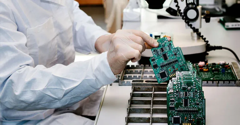
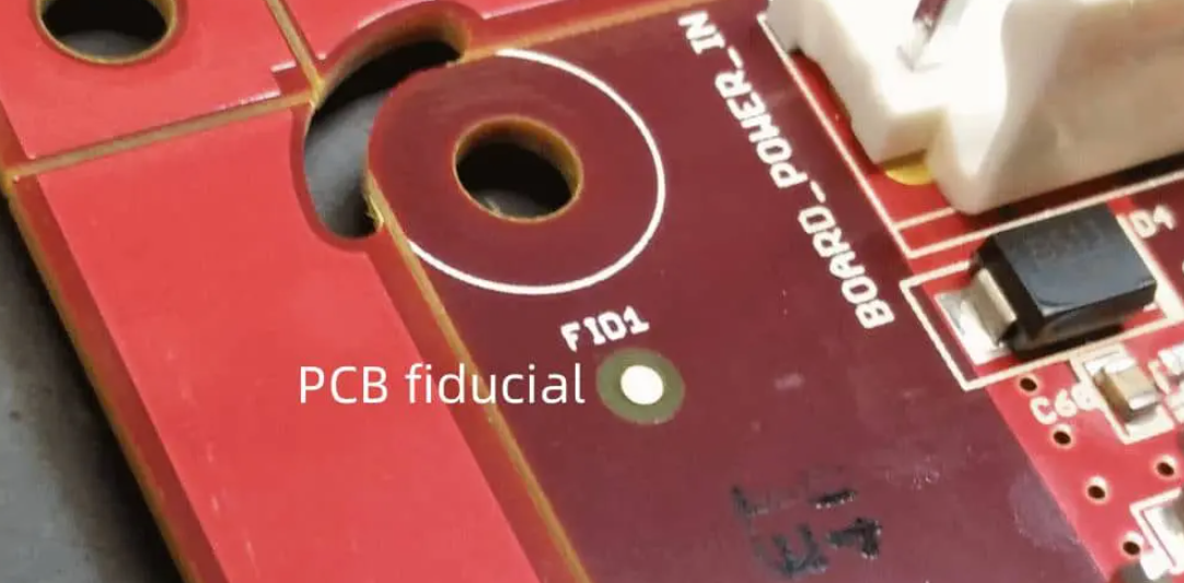
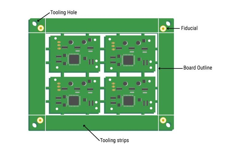
SMT alignment within a panelized setup relies on precise coordination between design, tooling, and assembly processes. The primary goal is to ensure that components are placed accurately on each board within the panel. This begins with the design phase, where fiducial marks are incorporated. Fiducials are reference points on the PCB that machines use to align components during SMT assembly. Typically, these marks are placed at the corners of each board within the panel to provide a clear reference for pick-and-place machines.
Another key principle is the stability of the panel during assembly. Panels must be designed to minimize movement or vibration, as even slight shifts can disrupt component alignment for efficient assembly. Tooling holes, often placed along the panel edges, help secure the panel in assembly equipment. These holes ensure the panel remains fixed during the placement and soldering processes. Without proper alignment mechanisms, components may deviate from their intended positions, leading to defects.
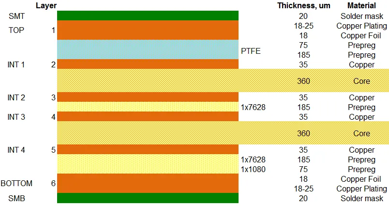
Warpage is another concern in panelized SMT assembly. If the panel bends or distorts under heat or mechanical stress, alignment accuracy suffers. Industry standards, such as IPC-6012E, provide guidelines on acceptable warpage limits to maintain precision during assembly. Hobbyists should consider material selection and panel thickness to reduce warpage risks, ensuring consistent alignment across all boards in the panel.
Best Practices for Component Alignment in Panelized Boards
Achieving component alignment for efficient assembly requires attention to several best practices. First, ensure that fiducial marks are clearly defined and positioned according to standard guidelines. These marks should be free from solder mask or other coverings to allow assembly machines to detect them accurately. For hobbyists working with limited equipment, manual alignment may be necessary, so placing additional visual reference points can help.
Second, consider the spacing between individual boards within the panel. Adequate spacing prevents interference during component placement and soldering. It also simplifies the application of correct panel breakout guidelines by reducing the risk of damage to adjacent boards during separation. A common practice is to include a border or rail around the panel edges to provide extra stability and handling space.
Third, verify the accuracy of your design files before manufacturing. Errors in the Gerber files, such as misaligned layers or incorrect fiducial placement, can lead to assembly issues. Double-check that all components are oriented correctly in the design software to match the intended layout on the physical panel. Following these steps ensures that component alignment supports efficient assembly, even in small-scale setups.
Correct Panel Breakout Guidelines for Hobbyists
After assembly, separating individual boards from the panel requires careful adherence to correct panel breakout guidelines. Improper breakout can damage traces, components, or board edges, rendering the PCB unusable. The two primary methods for panel separation are V-scoring and tab routing, each with specific considerations.
V-scoring involves creating shallow grooves along the separation lines during manufacturing. These grooves allow hobbyists to snap the boards apart manually. When using V-scored panels, apply even pressure along the score line to avoid stress on components near the edges. If the panel is thick or contains delicate parts, consider using a depaneling tool to minimize risk.
Tab routing, on the other hand, uses small perforated tabs to hold boards together within the panel. These tabs are broken during separation, often with a simple twisting motion. Ensure that tabs are placed away from sensitive areas to prevent damage. Industry standards like IPC-A-600K provide criteria for acceptable breakout quality, ensuring that edges remain clean and free from cracks after separation.
For hobbyists, always wear protective gear when breaking out panels, as small fragments may pose a hazard. Inspect each board after separation for any signs of damage, especially near the edges. Following correct panel breakout guidelines preserves the integrity of your assembled boards and prevents costly rework.
Machine Soldering Techniques for Panelized SMT Assembly
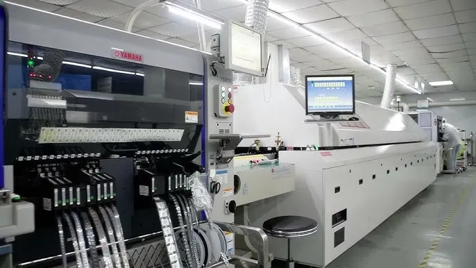
Machine soldering techniques are vital for achieving reliable connections on panelized SMT boards. The most common method is reflow soldering, where solder paste is applied to component pads, and the entire panel is heated in a reflow oven. This process melts the solder, forming strong bonds between components and the board. For hobbyists, access to a reflow oven may be limited, but small desktop ovens or hot plates can serve as alternatives.
Temperature control is critical during reflow soldering. Overheating can damage components or cause solder joints to fail, while insufficient heat may result in cold solder joints. Industry standards, such as IPC J-STD-020E, outline acceptable temperature profiles for different component types, ensuring safe and effective soldering. Hobbyists should follow a gradual heating and cooling curve to prevent thermal shock to the panel or components.
Another technique is wave soldering, though it is less common for SMT due to its focus on through-hole components. If combining SMT and through-hole parts on a panel, apply wave soldering only after SMT reflow to avoid disrupting surface-mounted components. Proper fixturing of the panel during soldering prevents movement, maintaining alignment throughout the process.
For small-scale projects, manual soldering may be necessary to correct defects after machine processes. Use a fine-tip soldering iron and apply minimal heat to avoid damaging nearby components. Following established machine soldering techniques ensures consistent results, even when working with limited resources.
Troubleshooting Common SMT Alignment Issues in Panelization
Alignment issues during SMT assembly of panelized boards can stem from several sources, and troubleshooting them is key for hobbyists. One common problem is fiducial mark detection failure. If assembly equipment cannot locate fiducials due to poor contrast or obstruction, components may be misplaced. Ensure fiducials are exposed and positioned per design specifications to resolve this issue.
Another frequent issue is panel warpage, which disrupts component alignment for efficient assembly. Warpage often occurs due to uneven heating or material stress. Test the panel flatness before assembly, and adhere to guidelines in IPC-6012E for acceptable limits. If warpage is detected, consider adjusting the panel design or using a different substrate material for future batches.
Component shift during reflow soldering is also a concern. This happens when solder paste melts unevenly, pulling components out of position. Verify that solder paste is applied uniformly and that the reflow profile matches recommendations in IPC J-STD-020E. For manual corrections, carefully reposition and resolder shifted components with minimal heat. Addressing these issues ensures reliable assembly outcomes.
Conclusion
Panelization and SMT alignment are foundational to achieving high-quality PCB assembly, even for electronic hobbyists working on small projects. By focusing on component alignment for efficient assembly, adhering to correct panel breakout guidelines, and applying proper machine soldering techniques, you can minimize defects and improve results. Understanding technical principles, following industry standards, and troubleshooting common issues empower hobbyists to tackle complex assembly tasks with confidence. Implementing the best practices discussed ensures that your panelized boards meet functional and quality expectations, paving the way for successful electronic projects.
FAQs
Q1: How does component alignment for efficient assembly impact SMT outcomes?
A1: Component alignment is crucial for successful SMT assembly as it ensures accurate placement on panelized boards. Misalignment can lead to soldering defects or electrical failures. Using fiducial marks and stable panel designs, as outlined in industry standards like IPC-6012E, helps achieve precision. Proper alignment reduces rework and enhances the reliability of the final product for hobbyists.
Q2: What are the correct panel breakout guidelines for separating PCBs?
A2: Correct panel breakout guidelines involve using V-scoring or tab routing for separation. Apply even pressure when snapping V-scored panels to avoid stress on components. For tab routing, break tabs carefully away from sensitive areas. Standards like IPC-A-600K provide criteria for clean edges, helping hobbyists prevent damage during breakout and maintain board integrity.
Q3: Which machine soldering techniques work best for panelized SMT boards?
A3: Reflow soldering is the primary technique for SMT on panelized boards, melting solder paste to form connections. Follow temperature profiles from IPC J-STD-020E to avoid thermal damage. For mixed assemblies, use wave soldering after reflow. Hobbyists can use desktop reflow ovens or hot plates to achieve consistent results with careful heat control.
Q4: How can hobbyists troubleshoot alignment issues during SMT panelization?
A4: Alignment issues often arise from undetected fiducials or panel warpage. Ensure fiducials are clear and follow design rules for visibility. Check panel flatness against IPC-6012E limits to prevent warpage. If components shift during soldering, verify solder paste application and reflow profiles per IPC J-STD-020E. These steps help resolve common alignment challenges.
References
IPC-6012E — Qualification and Performance Specification for Rigid Printed Boards. IPC, 2020.
IPC-A-600K — Acceptability of Printed Boards. IPC, 2020.
IPC J-STD-020E — Moisture/Reflow Sensitivity Classification for Nonhermetic Surface Mount Devices. IPC, 2014.