Introduction
High-frequency PCB assembly plays a critical role in modern electronics, especially in applications like telecommunications, radar systems, and high-speed digital devices. These assemblies must handle signals operating at gigahertz frequencies, where even minor design flaws can lead to significant performance issues. Key challenges include maintaining signal integrity, achieving precise impedance control, and selecting suitable materials to minimize signal loss. For electrical engineers, understanding these factors is essential to ensure reliable operation in demanding environments. This article explores the core design considerations and challenges of high-frequency PCB assembly, offering practical insights into material selection for high-frequency PCB, impedance management, and strategies for optimizing performance. The focus remains on technical precision and adherence to industry standards.
What Is High-Frequency PCB Assembly and Why It Matters
High-frequency PCB assembly refers to the process of designing, manufacturing, and assembling printed circuit boards that operate at frequencies typically above 100 MHz, often extending into the gigahertz range. These boards are fundamental in applications such as 5G networks, satellite communications, and automotive radar systems. The significance of high-frequency PCB assembly lies in its ability to support rapid data transmission and maintain signal quality under stringent conditions.
Unlike standard PCB designs, high-frequency assemblies demand meticulous attention to signal propagation, electromagnetic interference, and thermal management. A failure to address these aspects can result in signal degradation, increased noise, or complete system failure. For engineers, the stakes are high, as these boards often form the backbone of critical infrastructure. Ensuring robust performance through careful design and assembly practices is not just a technical requirement but a necessity for operational success.
Technical Principles of High-Frequency PCB Assembly
Signal Integrity in High-Frequency Designs
Signal integrity refers to the preservation of a signal’s quality as it travels through a PCB. At high frequencies, signals are prone to distortion due to reflections, crosstalk, and attenuation. Reflections occur when there is an impedance mismatch along the signal path, sending part of the signal back toward the source. Crosstalk arises when adjacent traces interfere with each other, introducing unwanted noise. Attenuation, or signal loss, happens due to dielectric losses and conductor resistance, which become more pronounced as frequency increases.
To maintain signal integrity, engineers must consider trace geometry, spacing, and termination techniques. Controlled impedance traces are vital to prevent reflections, while proper grounding and shielding reduce crosstalk. These principles form the foundation of high-frequency PCB design, ensuring that signals remain clear and reliable during transmission.
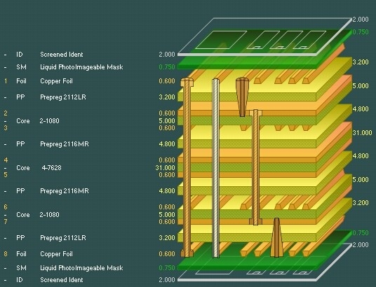
Impedance Control and Its Importance
Impedance control is a cornerstone of high-frequency PCB assembly. It involves designing transmission lines on the PCB to match the characteristic impedance of the system, typically 50 ohms for RF applications. Mismatched impedance leads to signal reflections, which degrade performance and can cause data errors in high-speed circuits.
Achieving impedance control requires precise calculation of trace width, thickness, and spacing, as well as the dielectric properties of the substrate material. The stack-up configuration also plays a role, as the proximity of ground planes affects the electromagnetic field around traces. Industry standards, such as IPC-2141A, provide guidelines for designing controlled impedance circuits, ensuring consistency and reliability in high-frequency applications.
Material Selection for High-Frequency PCB
Material selection for high-frequency PCB is a critical factor in minimizing signal loss and maintaining performance. Standard FR-4 materials, often used in low-frequency designs, are inadequate for high-frequency applications due to their high dielectric constant and loss tangent. These properties lead to greater signal attenuation and phase distortion at higher frequencies.
Instead, engineers often turn to specialized laminates with low dielectric constants and low loss tangents. Materials with stable dielectric properties over a wide frequency range are preferred to ensure consistent performance. Additionally, the thermal and mechanical stability of the material must be considered, as high-frequency circuits can generate significant heat. Selecting the right substrate is a balancing act between electrical performance, cost, and manufacturability.
Suggested Reading: High-Performance PCB Assembly: Key Design Considerations 2026
Challenges in High-Frequency PCB Assembly
Minimizing Signal Loss
Minimizing signal loss is a primary challenge in high-frequency PCBA assembly. Signal loss occurs due to conductor losses, dielectric losses, and radiation losses. Conductor losses are influenced by the skin effect, where high-frequency currents flow only on the surface of conductors, increasing effective resistance. Dielectric losses result from the energy absorbed by the substrate material, while radiation losses occur when electromagnetic energy escapes from the board.
To address these issues, engineers use wider traces or thicker copper to reduce conductor losses. Selecting low-loss dielectric materials helps mitigate dielectric losses. Additionally, proper shielding and grounding techniques prevent radiation losses. These strategies require careful planning during the design phase to ensure optimal signal transmission.
Managing Electromagnetic Interference
Electromagnetic interference, or EMI, poses a significant challenge in high-frequency designs. EMI can originate from external sources or from within the PCB itself due to closely spaced traces or poor grounding. At high frequencies, even small parasitic capacitances and inductances can amplify interference, disrupting signal integrity.
Effective EMI management involves implementing ground planes to provide a low-impedance return path for signals. Shielding sensitive components and traces also helps isolate them from external noise. Adhering to layout guidelines, such as avoiding long parallel traces, further reduces the risk of interference. These practices are essential for maintaining reliable operation in high-frequency environments.
Thermal Management Issues
High-frequency circuits often generate substantial heat due to rapid switching and power dissipation. Excessive heat can alter the dielectric properties of materials, leading to signal distortion or component failure. Thermal management becomes even more complex in compact designs where space for heat dissipation is limited.
Engineers address this challenge by incorporating thermal vias to transfer heat away from critical areas. Selecting materials with high thermal conductivity also aids in heat dissipation. In some cases, additional cooling mechanisms may be necessary to maintain optimal operating conditions. Proper thermal design is crucial to ensure the longevity and reliability of high-frequency assemblies.
Practical Solutions and Best Practices for High-Frequency PCB Assembly
Design Guidelines for Signal Integrity
Maintaining signal integrity starts with a well-planned layout. Keep high-frequency traces as short and direct as possible to minimize delay and loss. Use differential pairs for critical signals to reduce noise susceptibility. Ensure that ground planes are continuous beneath signal traces to provide a stable return path. Avoid vias in high-frequency signal paths, as they introduce inductance and capacitance that can distort signals.
Strategies for Impedance Control
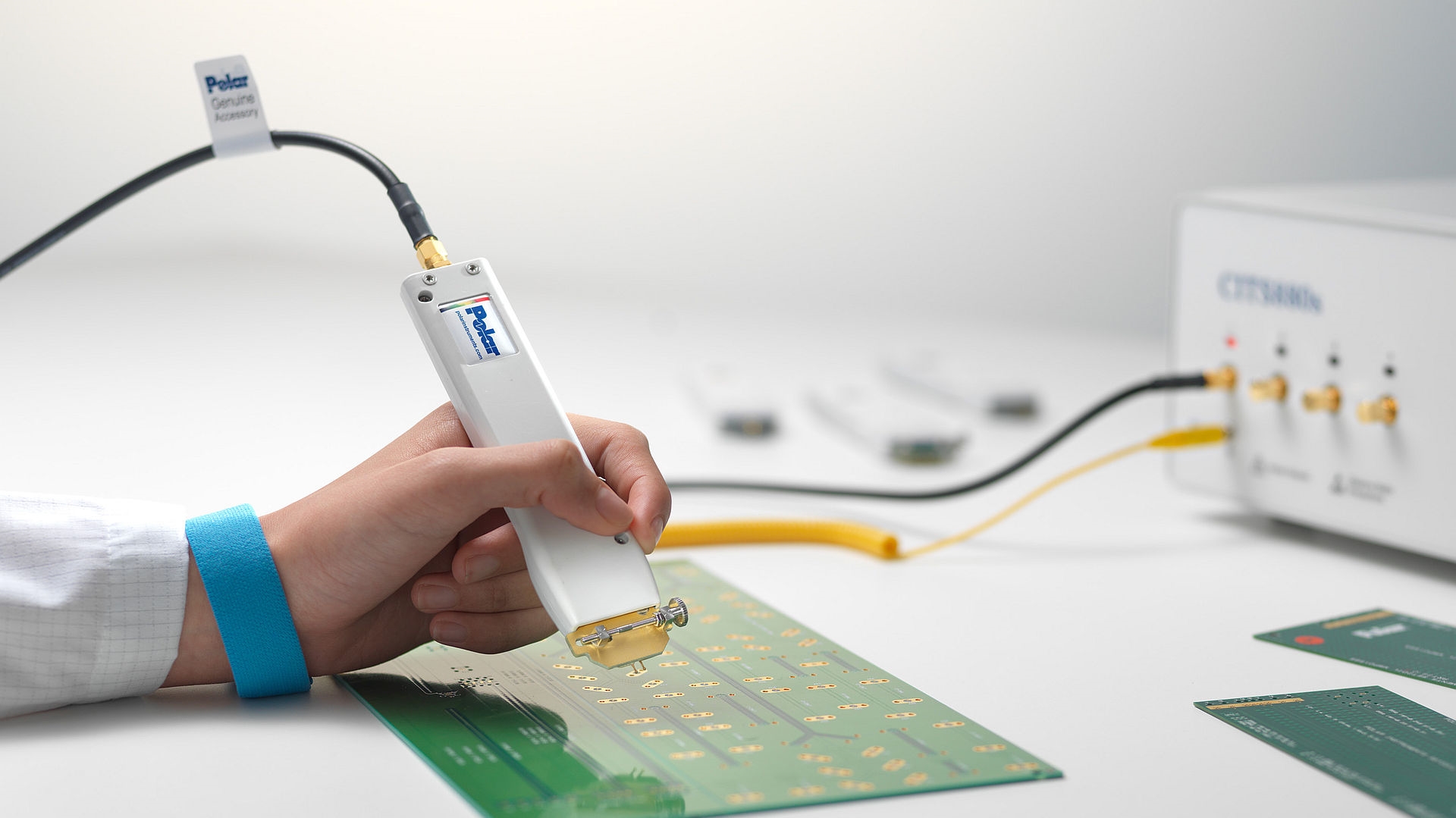
Achieving precise impedance control requires accurate modeling and simulation during the design phase. Calculate trace dimensions based on the desired impedance and the dielectric properties of the substrate. Use reference planes to maintain consistent impedance across the board. Regularly consult industry standards like IPC-2141A for guidance on controlled impedance design. Testing prototypes with time-domain reflectometry can help verify impedance matching before full-scale production.
Material Selection Tips
When choosing materials for high-frequency PCB, prioritize those with low dielectric constants and low loss tangents. Ensure that the material’s properties remain stable across the operating frequency range and temperature conditions. Consider the coefficient of thermal expansion to prevent mechanical stress during thermal cycles. Work closely with manufacturing teams to confirm that the selected material is compatible with assembly processes and meets performance requirements.
Assembly Techniques to Minimize Signal Loss
During assembly, maintain strict control over soldering processes to avoid introducing defects that could impact signal quality. Use reflow profiles that comply with standards like IPC/JEDEC J-STD-020E to prevent thermal damage to components and substrates. Inspect solder joints for consistency, as poor connections can increase resistance and signal loss. Additionally, handle boards with care to avoid mechanical stress that could alter trace geometry or material properties.
Troubleshooting Common Issues in High-Frequency PCB Assembly
For assembly engineers, identifying and resolving issues in high-frequency PCB assembly is a routine task. One common problem is signal reflection due to impedance mismatches. This can often be traced back to incorrect trace widths or inconsistent stack-up configurations. Using simulation tools to model impedance before fabrication can prevent such issues. Another frequent concern is excessive EMI, often caused by inadequate grounding. Adding ground vias near high-frequency components can resolve this problem.
Thermal hotspots are also a recurring issue, particularly in densely packed designs. If components overheat, consider redesigning the layout to improve airflow or add thermal vias. Always validate designs against standards like IPC-A-600K to ensure acceptability of the final board. These troubleshooting steps, grounded in practical experience, help maintain the performance of high-frequency assemblies under real-world conditions.
Conclusion
High-frequency PCB assembly presents unique challenges that demand precision in design and execution. From ensuring signal integrity to achieving impedance control, every aspect requires careful consideration. Material selection for high-frequency PCB is pivotal in minimizing signal loss, while effective thermal and EMI management ensures reliability. By following best practices and adhering to industry standards, engineers can overcome these challenges and deliver robust solutions for demanding applications. A thorough understanding of these principles equips teams to tackle the complexities of high-frequency designs with confidence.
FAQs
Q1: What are the key factors in maintaining signal integrity during high-frequency PCB assembly?
A1: Signal integrity in high-frequency PCB assembly depends on controlled impedance, proper grounding, and minimal trace lengths. Avoiding vias in signal paths and using continuous ground planes reduces noise and reflections. Spacing traces adequately prevents crosstalk. Following layout guidelines ensures signals remain undistorted during transmission.
Q2: How does material selection for high-frequency PCB impact performance?
A2: Material selection for high-frequency PCB directly affects signal loss and performance. Materials with low dielectric constants and loss tangents minimize attenuation and phase distortion. Stability across frequency and temperature ranges is crucial. Choosing the right substrate ensures reliable operation in high-frequency applications.
Q3: Why is impedance control critical in high-frequency PCB designs?
A3: Impedance control is vital in high-frequency PCB designs to prevent signal reflections that degrade performance. Matching trace impedance to system requirements, often 50 ohms, ensures signal quality. Precise trace dimensions and stack-up design are necessary. Standards like IPC-2141A provide essential guidance for success.
Q4: What are effective strategies for minimizing signal loss in high-frequency PCB assembly?
A4: Minimizing signal loss involves using low-loss materials and wider traces to reduce conductor losses. Proper shielding prevents radiation losses, while optimized layouts limit dielectric losses. Careful assembly techniques, adhering to standards like IPC-A-600K, ensure minimal defects that could impact signal quality.
References
IPC-2141A — Design Guide for High-Speed Controlled Impedance Circuit Boards. IPC, 2004.
IPC-A-600K — Acceptability of Printed Boards. IPC, 2020.
IPC/JEDEC J-STD-020E — Moisture/Reflow Sensitivity Classification for Nonhermetic Surface Mount Devices. IPC/JEDEC, 2014.


