Introduction
In high-frequency PCB design, maintaining signal integrity is paramount as data rates climb into the multi-gigabit per second range. Through-hole vias, essential for interconnecting multilayer boards, often introduce unwanted stubs that extend beyond the active signal layers. These stubs act as resonant elements, causing signal reflections, insertion loss, and degradation in overall performance. PCB back drilling emerges as a critical manufacturing technique to address these issues by selectively removing the unused portion of the via barrel. This process directly contributes to PCB back drilling benefits, enabling cleaner signal transmission in demanding applications like telecommunications and computing systems. Engineers must understand its principles to optimize designs for speed and reliability.
As board thicknesses increase to accommodate more layers, the stub length grows proportionally, exacerbating impedance mismatches and crosstalk. Traditional solutions like blind or buried vias add complexity and cost, making backdrilling a practical alternative for many scenarios. By focusing on via stub reduction, backdrilling supports impedance control and enhances high-frequency performance without redesigning the entire stackup. This article explores the mechanics, benefits, and implementation strategies, grounded in established manufacturing practices.
What Is PCB Back Drilling and Why It Matters
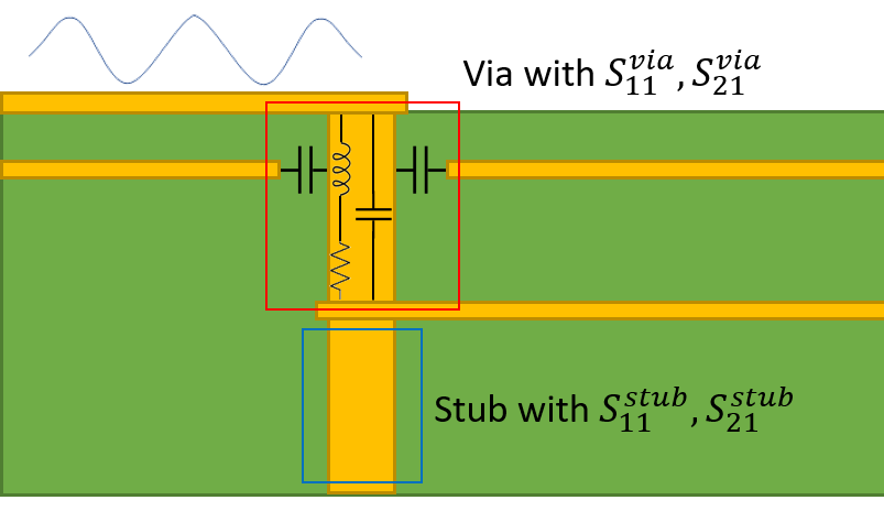
PCB back drilling involves using a larger-diameter drill bit from the opposite side of the board to remove the copper-plated stub of a through-hole via after the initial plating process. This controlled depth drilling targets only the non-functional portion, leaving the interconnection between intended layers intact. The technique requires precise alignment and depth control to avoid damaging active pads or traces. In essence, it transforms a standard through via into a functional equivalent of a blind via for signal paths.
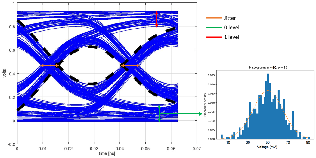
The relevance stems from the physics of high-speed signals, where wavelengths shorten dramatically, making even short stubs electrically long. At frequencies above several gigahertz, these stubs create open-circuit discontinuities that reflect portions of the signal backward, distorting the waveform. This leads to eye diagram closure, increased bit error rates, and compliance failures in high-frequency PCB design. PCB back drilling benefits become evident here, as stub removal minimizes these reflections, preserving signal quality over longer traces.
Factory-driven insights highlight its role in multilayer boards exceeding eight layers, where through vias are unavoidable for power and ground distribution. Without backdrilling, designers face trade-offs between layer count and performance. Standards like IPC-6012E outline qualification requirements for such features, ensuring reliability in production environments. Ultimately, it bridges design intent with manufacturable outcomes for signal integrity improvement.
Technical Principles of PCB Backdrilling
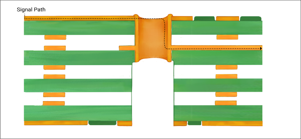
The core issue with through-hole vias lies in their electrical length. In a typical multilayer PCB, a via drilled from top to bottom connects all layers, but a signal routing between, say, layer 4 and layer 6 only uses the central portion. The remaining copper barrel on either end forms stubs that behave like transmission line resonators. At high frequencies, the stub's length approaches a quarter-wavelength, causing a pronounced impedance discontinuity and maximum reflection.
Backdrilling counters this by mechanically excavating the stub to a depth slightly beyond the last active land, typically leaving a small cleanup zone. This reduces the effective stub length to near zero for the signal path, minimizing return loss and insertion loss. Signal propagation models show that reflections coefficient decreases exponentially with stub shortening, directly aiding impedance control. For instance, the characteristic impedance of the via transitions more smoothly to the trace impedance, reducing mismatches.
Via stub reduction is quantifiable through time-domain reflectometry, where shorter stubs yield cleaner reflections in measurements. In high-frequency PCB design, this translates to wider eye openings and lower jitter. Crosstalk between adjacent vias also diminishes, as the stub no longer couples energy to neighboring structures. The process preserves plating integrity in the functional zone, maintaining mechanical strength per IPC-2221 guidelines for via design.
Electromagnetic simulations further validate these principles, demonstrating how backdrilled vias support data rates beyond 25 Gbps with minimal equalization needs. The annular ring around the backdrill must be sufficient to prevent breakthrough, influencing drill size selection. Depth tolerances ensure consistency across panels, critical for array-based production. Overall, these mechanisms underpin signal integrity improvement in real-world boards.
Key PCB Back Drilling Benefits for High-Frequency Applications
One primary PCB back drilling benefit is enhanced signal integrity improvement through drastic via stub reduction. By eliminating resonant stubs, signals experience less attenuation and distortion, crucial for maintaining data integrity in backplanes and SerDes channels. Engineers observe improved return loss profiles, often exceeding 20 dB across the operating band in optimized designs.
Impedance control sees significant gains, as the via's inductive and capacitive reactance align better with trace values. This uniformity reduces the need for aggressive de-embedding in simulations, streamlining design verification. In dense routing, backdrilling mitigates near-end and far-end crosstalk, allowing tighter via spacing without performance penalties.
High-frequency PCB design benefits extend to reduced electromagnetic interference, as cleaner signals radiate less noise. Power integrity also improves indirectly, with ground vias backdrilled to minimize parasitic paths. Cost-wise, it avoids the premium of advanced via structures like microvias, offering a balanced solution for mid-to-high layer counts. These advantages make backdrilling indispensable for evolving standards in computing and networking.
Best Practices for PCB Backdrilling in Design and Manufacturing
Start with stackup planning to identify vias needing backdrilling, prioritizing those in critical high-speed nets. Specify backdrill depths in fabrication drawings, accounting for board thickness variations and drill entry offsets. Aim for stub remnants under 10 mils post-backdrill, with annular ring clearances per IPC-A-600K acceptability criteria. Use distinct drill symbols in tooling to differentiate standard and backdrill hits.
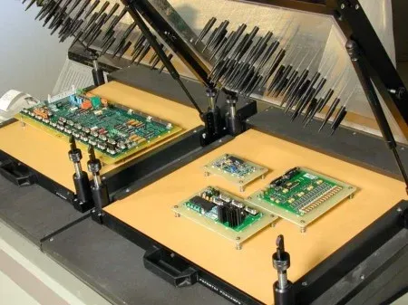
In manufacturing, employ controlled depth drilling with optical registration for alignment accuracy. Larger drill diameters, typically 10-20% bigger than the via, ensure complete stub removal without excessive enlargement of the functional barrel. Post-backdrill plating or etch-back may be needed to smooth shoulders, preventing solder wicking issues. Panel-level coupons validate depth uniformity, as required by IPC-6012E for performance qualification.
Inspection protocols include cross-sectioning sample vias and electrical testing for continuity and impedance. Tolerances for depth should not exceed ±5 mils for precision work, monitored via automated optical systems. Designers should simulate backdrill effects early, adjusting pad sizes to accommodate tolerances. Collaboration between design and fab teams ensures feasibility, avoiding costly respins.
Common Challenges and Troubleshooting in Backdrilling
Alignment errors can occur if registration between top and bottom drills drifts, leading to incomplete stub removal or pad damage. Mitigate with fiducials and machine vision, maintaining positional accuracy under 2 mils. Board warpage during thick panel drilling exacerbates this; use fixtures and sequential processing to flatten.
Over-drilling risks thinning the functional via wall, compromising current capacity. Conservative depth specs and pilot coupons prevent this. Residue from backdrilling may cause shorts if not desmeared properly, addressed via plasma cleaning. Electrical opens post-assembly signal plating inconsistencies in the shoulder region.
Troubleshooting starts with failure analysis via microsectioning, correlating defects to process parameters. Adjusting feed rates and spindle speeds optimizes hole quality. For high-volume runs, statistical process control tracks depth variations across panels.
Conclusion
PCB back drilling stands as a proven method to unlock high-frequency performance by addressing via stub limitations head-on. Its PCB back drilling benefits, including signal integrity improvement, via stub reduction, and precise impedance control, enable robust high-frequency PCB design. By integrating best practices and standards like IPC-6012E, engineers can achieve reliable outcomes in complex multilayer boards. As signal speeds escalate, backdrilling will remain a cornerstone technique, balancing performance, cost, and manufacturability for future innovations.
FAQs
Q1: What are the main PCB back drilling benefits for high-frequency PCB design?
A1: PCB back drilling benefits include via stub reduction, which minimizes signal reflections and improves insertion loss. It enhances impedance control by smoothing transitions, reducing crosstalk in dense layouts. Signal integrity improvement supports higher data rates without advanced via types, ideal for multilayer boards in telecom and servers. Factory processes ensure depth precision for consistent performance.
Q2: How does backdrilling contribute to signal integrity improvement?
A2: Backdrilling removes unused via stubs that cause quarter-wave resonances at high frequencies, leading to cleaner waveforms. This via stub reduction lowers return loss and jitter, widening eye openings in time-domain measurements. Impedance control improves as discontinuities vanish, aiding compliance in high-speed channels. Practical for boards over 10 layers, it aligns with IPC standards for qualification.
Q3: Why is via stub reduction critical in impedance control?
A3: Via stubs create inductive discontinuities, mismatching trace impedance and causing reflections. Backdrilling shortens stubs to negligible lengths, maintaining uniform impedance profiles across the signal path. This supports high-frequency PCB design by reducing equalization needs and EMI. Manufacturing tolerances ensure reliable stub elimination without weakening structures.
Q4: When should electrical engineers specify backdrilling in PCB designs?
A4: Specify backdrilling for high-speed nets in thick multilayer boards where through vias dominate. Target frequencies above 5 GHz or data rates over 10 Gbps for maximum gains. Review stackups for stub lengths exceeding signal rise times. Coordinate with fabs for tooling feasibility, leveraging standards for specs.
References
IPC-6012E — Qualification and Performance Specification for Rigid Printed Boards. IPC, 2015
IPC-2221B — Generic Standard on Printed Board Design. IPC, 2012
IPC-A-600K — Acceptability of Printed Boards. IPC, 2020