Introduction
In multilayer printed circuit boards designed for high-speed applications, vias serve as critical interconnects between layers, but traditional through-hole vias often introduce signal integrity issues due to their extended stubs. These stubs create impedance mismatches that lead to reflections, crosstalk, and insertion loss, particularly at frequencies above several gigahertz. PCB back drilling emerges as a targeted solution by selectively removing the unused portion of the via barrel, minimizing these effects without the need for complex layer buildup processes. In contrast, blind vias connect an outer layer to one or more inner layers without penetrating the entire board, while buried vias link only inner layers, both inherently avoiding full-height stubs. This PCB back drilling comparison highlights key differences in performance, cost, and manufacturability, helping electrical engineers make informed via selection decisions during PCB design trade-offs. Understanding these options ensures optimized signal paths in dense, high-performance designs.
Fundamentals of Vias in Multilayer PCBs
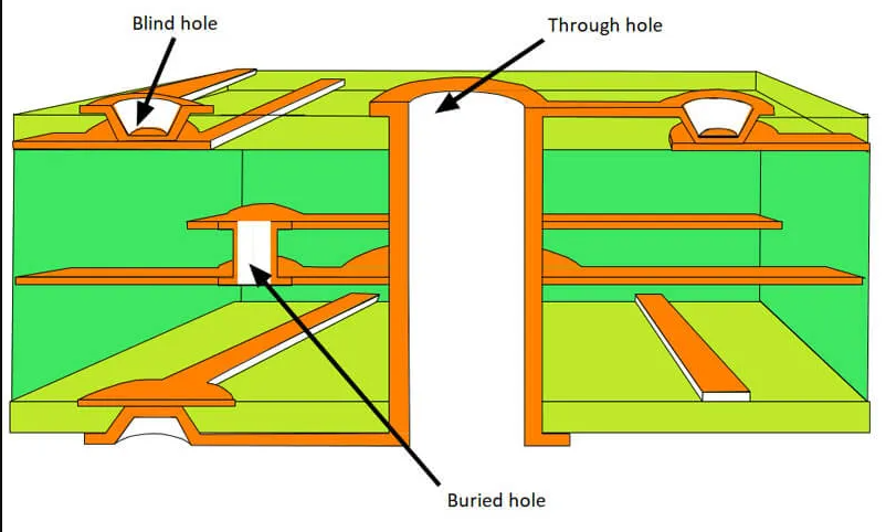
Vias form the backbone of interlayer communication in printed circuit boards, enabling routing flexibility in multilayer stackups. A standard through-hole via traverses the entire board thickness, providing reliable plating for conductivity but leaving a stub beyond the target layer that acts as a resonant transmission line element. Blind vias, as defined in design guidelines like IPC-2221, start from an outer layer and terminate at a specific inner layer, conserving board real estate and eliminating stubs on unused portions. Buried vias connect two or more inner layers exclusively, invisible from the surfaces, which supports dense inner routing planes. Each type influences board density, signal propagation, and fabrication yield, making via selection a pivotal aspect of PCB design trade-offs. Engineers must balance these characteristics against application requirements, such as data rates and layer count.
What is PCB Back Drilling?
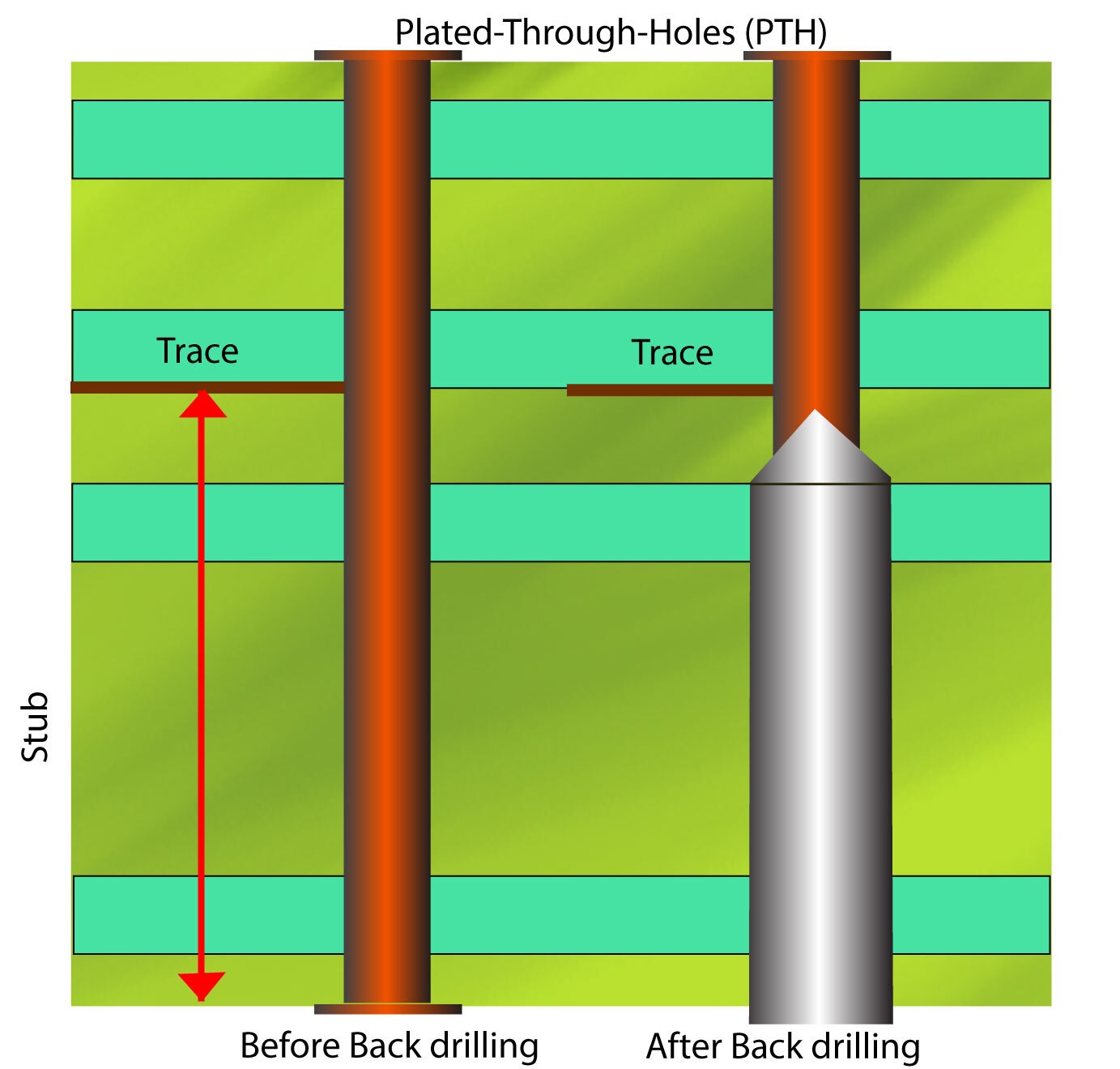
PCB back drilling involves a secondary drilling step after through-hole via formation and plating, where a larger diameter bit removes the stub from the opposite side of the board. This process shortens the effective via length to match the signal path needs, reducing parasitic inductance and capacitance that degrade high-speed signals. The backdrill diameter typically exceeds the primary via drill by 0.1 to 0.2 mm to ensure complete stub removal without damaging the plated barrel. Fabricators control depth precisely using optical or mechanical methods, aligning with performance specifications in IPC-6012 for rigid boards. This technique proves especially valuable in boards exceeding 10 layers, where full blind or buried via implementation becomes prohibitively complex. By preserving the integrity of the conductive path while truncating unnecessary sections, back drilling offers a practical enhancement to standard through vias.
Technical Principles of Blind and Buried Vias
Blind vias require controlled-depth drilling or laser ablation from the surface, followed by sequential lamination to build layers around the partially plated structure. This method avoids stubs entirely for the connected layers but demands precise registration between build cycles to prevent misalignment. Buried vias form during inner core lamination, fully enclosed within the stackup, which optimizes plane continuity and minimizes surface clutter. Both types support finer pitches than through vias, aiding high-density interconnects, though they introduce challenges in thermal management and plating uniformity. Signal propagation benefits from shorter paths and consistent impedance, crucial for maintaining eye diagrams in gigabit Ethernet or DDR memory interfaces. Compared to back drilling, these vias demand more process steps, yet they excel in applications prioritizing routing density over fabrication simplicity.
Signal Integrity Comparison: Blind Vias vs Back Drilling and Buried Vias
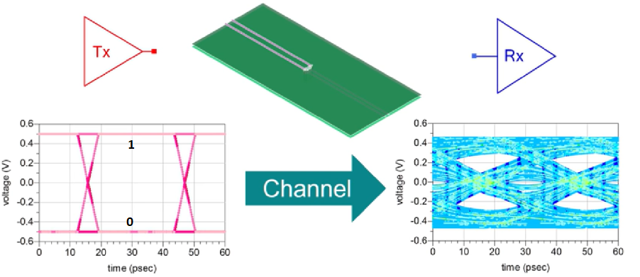
Through-via stubs longer than one-tenth the signal rise time equivalent length introduce significant return loss, often exceeding 10 dB at multi-GHz frequencies. Back drilling mitigates this by targeting stub lengths below 5 mm in typical stackups, preserving most of the plated via for mechanical strength. Blind and buried vias eliminate stubs by design, offering superior insertion loss performance in HDI structures, but their smaller apertures limit current carrying capacity compared to backdrilled vias. Crosstalk reduces across all options versus full through vias, with buried vias providing the best isolation due to full encapsulation. Simulations using field solvers reveal that backdrilled vias match blind via performance in 80 percent of cases for data rates up to 25 Gbps, per common engineering analyses. Thus, buried vias vs back drilling trade-offs center on whether inner-layer density justifies added cost.
Key aspects summarized by via type:
Back Drilling
- Stub Length: Controlled removal
- Signal Integrity: Excellent for high layers
- Manufacturing Cost: Low to moderate
- Density Benefit: Moderate
- Layer Compatibility: Any through via
Blind Vias
- Stub Length: None
- Signal Integrity: Superior for surface connects
- Manufacturing Cost: High
- Density Benefit: High
- Layer Compatibility: Outer to inner
Buried Vias
- Stub Length: None
- Signal Integrity: Best for inner routing
- Manufacturing Cost: High
- Density Benefit: Highest
- Layer Compatibility: Inner only
Manufacturing and Cost Trade-offs
Back drilling integrates into standard through-hole processes, adding only a post-plating drill and clean step, which keeps costs 20 to 50 percent lower than blind or buried vias for prototypes. Blind vias necessitate multiple lamination cycles, increasing yield risks from core warping and alignment errors, while buried vias embed in cores but multiply buildup expenses. IPC-6012 outlines acceptance criteria for backdrill depth control and surface roughness, ensuring reliability comparable to unmodified vias. Fabricators prefer back drilling for volumes under 1000 units due to simpler tooling, whereas blind and buried suit production runs where density offsets premium pricing. Engineers should specify backdrill margins in fabrication notes to avoid over-etching the barrel. Overall, PCB design trade-offs favor back drilling for cost-sensitive high-speed boards without extreme miniaturization.
Best Practices for Via Selection in PCB Design
Start with signal integrity simulations to quantify stub impact, prioritizing back drilling where reflections exceed margins. For blind vias, allocate adequate annular ring per layer pairing, and stagger vias to distribute thermal stress. Buried vias benefit from dedicated inner signal layers, enhancing ground return paths. Document backdrill depths and diameters in stackup drawings, targeting 10 percent overshoot tolerance. Validate designs with coupon structures for depth and plating checks during fabrication. Combine techniques, such as backdrilled through vias alongside buried for hybrid optimization. These practices align via selection with performance goals while respecting manufacturability limits.
Case Study: High-Speed SerDes Interface Design
Consider a 16-layer PCB for a 56 Gbps SerDes transceiver, where through-via stubs caused 15 dB return loss at 28 GHz. Implementing back drilling on critical nets reduced stubs to 2 mm, improving eye height by 30 percent without stackup changes. Alternative blind vias on surface layers freed routing space but doubled lead time due to sequential build. Buried vias handled inner differential pairs effectively, minimizing crosstalk to below 40 dB. This PCB back drilling comparison demonstrated 40 percent cost savings versus full blind/buried adoption, validating hybrid via strategies for balanced trade-offs. Post-assembly tests confirmed compliance with impedance targets across all nets.
Conclusion
Selecting between PCB back drilling, blind vias, and buried vias hinges on balancing signal integrity, density, cost, and manufacturing feasibility in your specific design. Back drilling provides a versatile, economical path for stub mitigation in complex stackups, while blind and buried vias unlock superior density for HDI applications. By evaluating PCB design trade-offs through simulation and standards adherence, engineers achieve robust performance without unnecessary complexity. Prioritize via selection early to streamline prototyping and production, ensuring your board meets high-speed demands efficiently.
FAQs
Q1: What is the main advantage of blind vias vs back drilling in PCB design?
A1: Blind vias vs back drilling offers complete stub elimination from outer to inner layers, ideal for high-density routing where surface space is premium. Back drilling modifies existing through vias cost-effectively but leaves a shortened barrel that may introduce minor roughness. Choose blind for compact HDI boards requiring precise impedance control, while back drilling suits retrofits on multilayer designs. This via selection optimizes signal paths based on layer access needs.
Q2: How does buried vias vs back drilling impact manufacturing costs?
A2: Buried vias vs back drilling increases costs due to inner core lamination and registration challenges, often 2-3 times higher for complex stackups. Back drilling adds minimal steps to standard processes, making it preferable for high-volume production. Both enhance signal integrity, but buried excels in inner plane integrity. Factor PCB design trade-offs like yield and lead time during budgeting.
Q3: When should electrical engineers prefer PCB back drilling in via selection?
A3: Opt for PCB back drilling comparison when layer counts exceed 12 and cost constraints limit sequential lamination for blind or buried vias. It effectively controls stubs for frequencies up to 50 GHz in rigid boards. Verify tolerances align with fabrication capabilities to avoid reliability issues. This approach balances performance and economy in demanding applications.
Q4: What are key PCB design trade-offs between these via types?
A4: PCB design trade-offs involve density versus simplicity: back drilling boosts signal integrity affordably but requires depth control, blind vias maximize surface efficiency at higher cost, and buried vias prioritize inner routing isolation. Simulate impacts on crosstalk and loss early. Standards guide implementation for consistent results across prototypes.
References
IPC-6012E — Qualification and Performance Specification for Rigid Printed Boards. IPC, 2017
IPC-2221B — Generic Standard on Printed Board Design. IPC, 2012
IPC-2226A — Sectional Design Standard for High Density Interconnect (HDI) Printed Boards. IPC, 2019


