Introduction
Electromagnetic compatibility (EMC) ensures that electronic devices operate without causing or suffering unacceptable electromagnetic interference. In printed circuit board (PCB) design, component placement directly influences EMC performance by controlling how signals couple between circuits. Poor placement can lead to radiated or conducted emissions that fail compliance tests, while optimized layouts minimize these risks. Electric engineers focus on EMC component placement to achieve reliable, interference-free operation in dense boards. This article explores strategies for reducing interference on PCBs through thoughtful component arrangement. Key principles and best practices enable compliance with industry standards from the outset.
Understanding EMC Component Placement and Its Importance
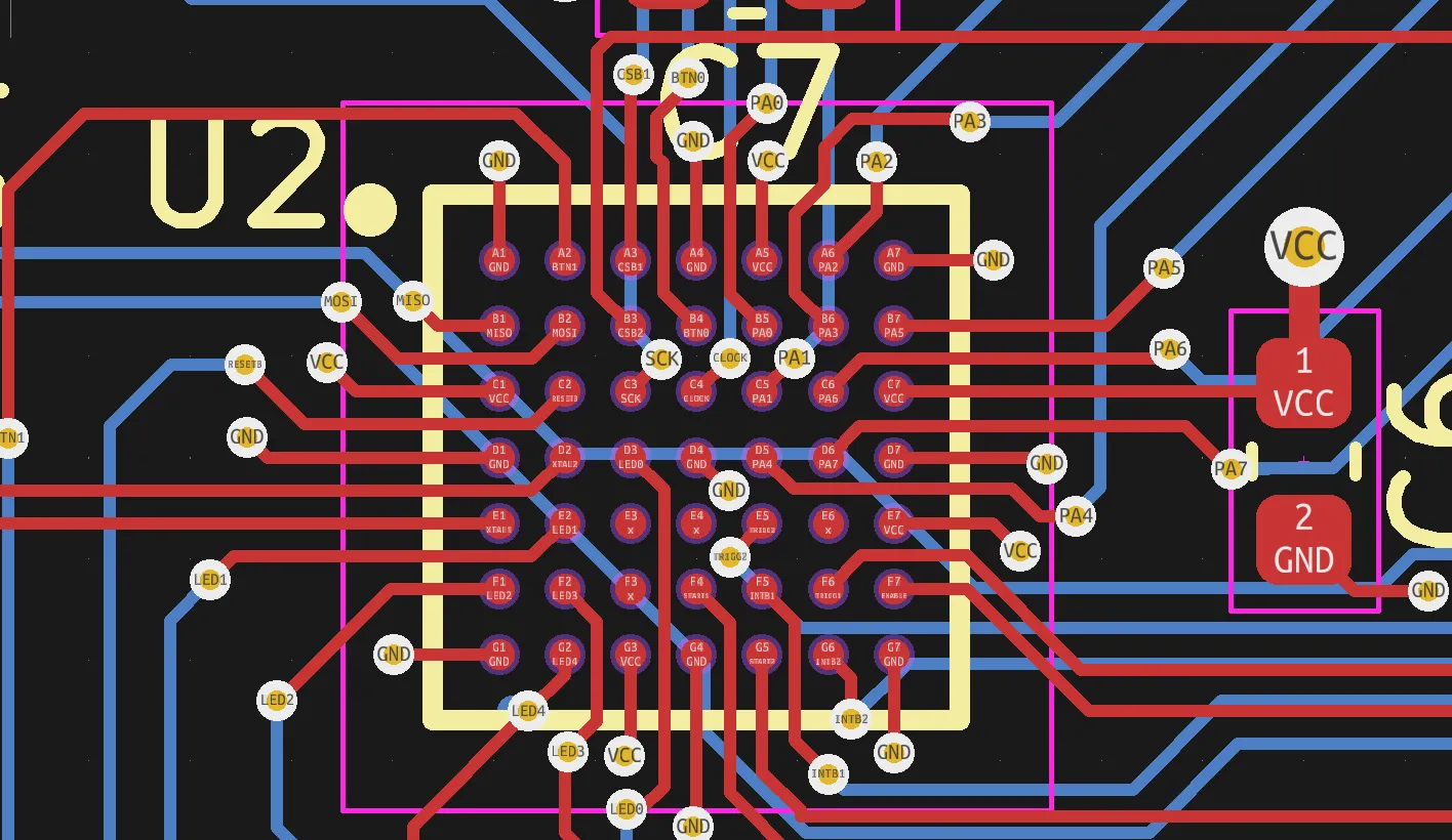
EMC component placement refers to the strategic positioning of active and passive components on a PCB to limit electromagnetic interference (EMI). Interference arises when energy from one circuit unintentionally affects another, degrading signal integrity or causing malfunctions. Effective placement reduces coupling paths, such as those between high-speed digital signals and analog sections. In high-density designs, this approach prevents issues like crosstalk or ground bounce that compromise overall system performance.
The relevance of component placement for electromagnetic compatibility grows with increasing clock speeds and integration levels in modern electronics. Devices must meet regulatory limits on emissions and susceptibility to pass certification, avoiding costly redesigns. Engineers prioritize this during layout to balance thermal, mechanical, and electrical constraints. Compliance not only satisfies legal requirements but also enhances product reliability in noisy environments like industrial or automotive applications. Neglecting it can result in field failures, underscoring the need for systematic design methodologies.
Technical Principles of Interference in PCB Layouts
Electromagnetic interference on PCBs occurs through capacitive, inductive, and radiated coupling mechanisms. Capacitive coupling transfers noise via electric fields between nearby traces or components, especially at high frequencies. Inductive coupling induces voltages in loops formed by current paths, amplifying when return currents stray far from sources. Radiated emissions propagate from antennas created by long traces or poor grounding, coupling into susceptible circuits.
Component placement influences these mechanisms by defining proximity and orientation. For instance, placing a switching regulator near an analog sensor increases common-mode noise through shared ground paths. Clock oscillators generate strong harmonics that radiate if positioned near board edges without shielding. Ground planes provide low-impedance returns, but partitions are needed to isolate sections, as per guidelines in IPC-2221. Understanding field patterns helps predict and mitigate risks during simulation.
Loop area minimization is central to reducing magnetic coupling. Large loops between signal and return paths act as efficient radiators, with area proportional to emission strength. Orienting components to shorten these loops, such as aligning vias directly under IC pins, cuts inductance. Electric field coupling decreases with physical separation, following the inverse square law for far-field effects. These principles guide placement decisions for electromagnetic compatibility.
Best Practices for EMC Component Placement
Start with functional grouping to separate noisy from sensitive components. Position digital logic and power converters on one side of the board, while analog circuits occupy the opposite. This isolation reduces crosstalk, with a minimum separation of several millimeters depending on frequencies involved. Place high-speed clocks centrally, away from I/O connectors to limit edge radiation.
Decoupling capacitors must sit as close as possible to power pins of integrated circuits, ideally within 1-2 mm. This forms a low-inductance path to shunt high-frequency noise to ground before it spreads. Use multiple values in parallel for broadband suppression, placed symmetrically around the chip. For mixed-signal devices, dedicate separate analog and digital decoupling to prevent noise bleed.
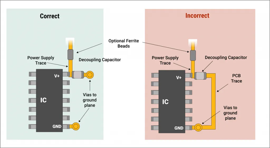
Implement solid ground and power planes beneath critical sections. Components over these planes benefit from image currents that cancel far-field radiation. Partition grounds at single points under mixed-signal ICs to avoid ground loops, stitching with vias nearby. Route signals parallel to planes rather than perpendicular to minimize fringing fields.
For I/O interfaces, centralize connectors on one board edge and surround them with filters. Place common-mode chokes and ferrites immediately adjacent to reduce conducted emissions. Sensitive inputs like ADCs should have dedicated guards or shields, grounded components acting as barriers. These practices align with IEC standards for emission limits.
Shielding cans over noisy elements like crystals or RF modules contain fields effectively. Ensure shields connect to ground at multiple points for low impedance across frequencies. In multilayer boards, bury high-speed traces between planes, placing surface components strategically.
Troubleshooting Common EMC Placement Issues
Engineers often encounter emissions from unoptimized clock placement near edges. Relocate oscillators inward and add ground vias around them to form a Faraday cage effect. Another issue arises in power sections where bypass caps are too distant, allowing ripple to propagate. Audit layouts with field solvers to quantify improvements post-adjustment.
Crosstalk in dense arrays stems from parallel traces without guards. Insert grounded traces between victims and aggressors, or reroute orthogonally. Susceptibility tests reveal pickup on unshielded sensors; add metal lids and twisted pairs for inputs. Iterative simulation verifies compliance before fabrication.
Conclusion
Strategic EMC component placement forms the foundation of interference-free PCB designs. By grouping functions, minimizing loops, and leveraging planes, engineers achieve robust electromagnetic compatibility. These methods reduce redesign cycles and ensure regulatory pass. Integrating principles early yields reliable products. Focus on proximity, partitioning, and shielding for optimal results.
FAQs
Q1: What is the primary goal of EMC component placement in PCB design?
A1: EMC component placement aims to minimize electromagnetic interference by separating noise sources from sensitive circuits. This involves positioning high-speed components centrally and analog sections remotely. Ground partitioning and close decoupling further suppress coupling. Compliance with standards like IPC-2221 supports these strategies for reliable operation.
Q2: How does reducing interference on PCBs improve product performance?
A2: Reducing interference on PCBs prevents signal degradation and false triggering in digital systems. Optimized layouts cut emissions, passing EMC tests on first try. This enhances immunity in harsh environments, extending device lifespan. Practical placement rules like I/O filtering yield measurable noise reductions.
Q3: Why place decoupling capacitors near ICs for electromagnetic compatibility?
A3: Decoupling capacitors near ICs provide local energy storage, bypassing high-frequency noise to ground. Short paths limit inductance, crucial for fast edges. This practice in component placement for electromagnetic compatibility stops ripple from affecting other circuits. Multiple caps cover wide frequency ranges effectively.
Q4: What role do ground planes play in EMC component placement?
A4: Ground planes offer low-impedance returns, shrinking loop areas and shielding signals. Place components over continuous planes to leverage image plane effects. Partitions isolate domains without loops. This foundational element supports overall EMC compliance in multilayer boards.
References
IPC-2221B — Generic Standard on Printed Board Design. IPC, 2012
IPC-6012E — Qualification and Performance Specification for Rigid Printed Boards. IPC, 2017
IEC 61000-6-4 — Electromagnetic compatibility (EMC) - Part 6-4: Generic standards - Emission standard for industrial environments. IEC, 2006
J-STD-001G — Requirements for Soldered Electrical and Electronic Assemblies. IPC, 2011