Introduction
Power electronics play a critical role in modern industries, from renewable energy systems to electric vehicles. Designing printed circuit boards (PCBs) for these applications requires careful attention to thermal management and reliability. High power densities lead to significant heat generation, which can compromise component performance and board longevity if not addressed. Key considerations such as power PCB layout, thermal management power strategies, copper weight power specifications, component placement power optimization, and creepage and clearance power requirements are essential for success. This article explores the principles and best practices for designing PCBs that handle high power loads effectively. Aimed at electrical engineers, the content provides structured insights into mitigating thermal challenges and ensuring compliance with industry standards for robust and reliable designs.
Why Thermal Management and Reliability Matter in Power Electronics
Power electronics involve circuits that handle high currents and voltages, often resulting in substantial heat dissipation. Without proper thermal management power strategies, excessive temperatures can degrade components, reduce efficiency, and cause system failures. Reliability is equally critical, as power systems are often deployed in demanding environments where downtime is costly. A well-designed power PCB layout addresses these challenges by optimizing heat dissipation and ensuring electrical safety. Standards from organizations like IPC and IEC provide guidelines to maintain performance and safety. Ignoring these aspects can lead to thermal runaway, component burnout, or insulation breakdown due to inadequate creepage and clearance power distances. Prioritizing these factors during design ensures long-term functionality and compliance with industry expectations.
Technical Principles of Heat Generation in Power Electronics PCBs
Heat in power electronics PCBs primarily arises from resistive losses in conductive traces and components, as well as switching losses in semiconductors. High current densities in traces with insufficient copper weight power ratings generate heat through Joule heating. Similarly, power components like MOSFETs and IGBTs produce heat during rapid switching due to energy dissipation. Thermal resistance between components and heat sinks or PCB layers further exacerbates temperature rise if not managed. Poor component placement power decisions can create hotspots by clustering heat-generating parts without adequate spacing for airflow or heat dissipation. Additionally, inadequate creepage and clearance power distances may lead to arcing or insulation failure under thermal stress, compounding reliability issues. Understanding these mechanisms is fundamental to designing effective solutions.
Key Factors Influencing Thermal Management and Reliability
Several design elements directly impact the thermal performance and reliability of power PCBs. Below are the critical factors electrical engineers must consider.
- Copper Weight Power Specifications: Thicker copper layers reduce resistance and improve heat spreading. Common weights range from 1 oz/ft2 to 3 oz/ft2 or higher for power applications, depending on current requirements.
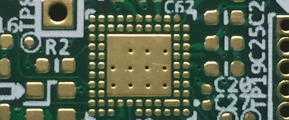
- Power PCB Layout Design: Strategic trace routing and layer stacking enhance heat dissipation. Wider traces and thermal vias connect heat-generating areas to dissipation layers.
- Component Placement Power Optimization: Distributing high-power components evenly prevents localized heating. Placing them near heat sinks or board edges aids cooling.
- Thermal Management Power Techniques: Incorporating heat sinks, thermal pads, and forced air cooling mitigates temperature rise. PCB materials with high thermal conductivity also help.
- Creepage and Clearance Power Requirements: Maintaining proper spacing between high-voltage traces prevents arcing and ensures safety, especially under thermal expansion.
Practical Solutions for Effective PCB Design in Power Electronics
Optimizing Copper Weight for Power Applications
Selecting the appropriate copper weight power rating is vital for handling high currents and dissipating heat. Thick copper PCB reduces electrical resistance, minimizing heat generation in traces. For power electronics, engineers often specify 2 oz/ft2 or higher, especially for traces carrying significant current. This choice must balance cost and thermal performance, as excessive copper increases manufacturing complexity. Standards like IPC-2221 provide guidelines for trace width and copper thickness based on current and temperature rise limits. Using multiple layers with heavy copper can also distribute current and heat more evenly across the board.
Strategic Power PCB Layout Techniques
A robust power PCB layout focuses on minimizing thermal and electrical stress. Engineers should route high-current traces as short and wide as possible to reduce resistance. Incorporating thermal vias near heat-generating components allows heat transfer to inner or bottom layers for dissipation. Ground planes on multiple layers act as heat spreaders while improving electrical stability. Standards such as IPC-2221 offer detailed recommendations on trace spacing and layer configurations to ensure thermal and electrical integrity. Simulation tools can help predict thermal behavior during the layout phase.
Component Placement for Power Efficiency
Effective component placement power strategies prevent thermal bottlenecks. High-power components should be spaced apart to avoid concentrated heat zones. Positioning them near board edges or heat sinks facilitates natural or forced convection. Sensitive components, like capacitors, must be placed away from heat sources to prevent degradation. Aligning components with airflow paths in the system enclosure further enhances cooling. Following guidelines from IPC-A-600K ensures that placement meets manufacturability and reliability criteria, reducing risks during assembly and operation.
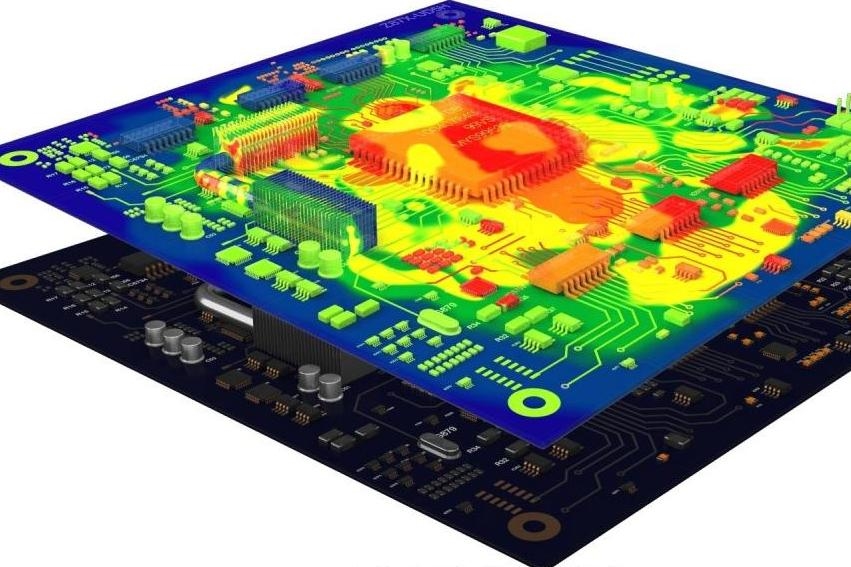
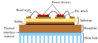
Thermal Management Power Strategies
Implementing thermal management power solutions is critical for high-power designs. Heat sinks attached to major heat sources, such as power transistors, can significantly lower operating temperatures. Thermal interface materials improve heat transfer between components and sinks. Forced air cooling or liquid cooling may be necessary for extreme power densities. Using PCB substrates with higher thermal conductivity, as recommended by JEDEC standards like J-STD-020E, supports better heat distribution. Regular thermal testing during PCB prototype manufacturing validates the effectiveness of these measures.
Ensuring Creepage and Clearance for Power Safety
Creepage and clearance power distances are essential for preventing electrical breakdown in high-voltage designs. Creepage refers to the shortest path along a surface between conductive parts, while clearance is the shortest distance through air. Both must account for voltage levels, environmental conditions, and thermal expansion. Standards like IEC 60950-1 provide specific spacing requirements based on voltage ratings and pollution degrees. For instance, higher altitudes or humid environments demand larger distances to prevent arcing. Proper design ensures safety and compliance with regulatory expectations.
Troubleshooting Common Issues in Power PCB Designs
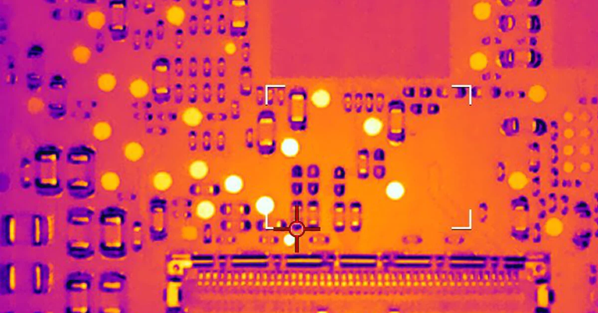
Thermal and reliability issues often surface during testing or operation of power electronics PCBs. Hotspots near high-power components indicate poor component placement power decisions or insufficient thermal vias. Engineers can address this by redistributing components or adding vias per IPC-2221 guidelines. Excessive trace heating suggests inadequate copper weight power specifications, requiring a shift to thicker copper or wider traces. Arcing or insulation failures point to insufficient creepage and clearance power distances, which must be corrected by adjusting trace spacing per IEC standards. Iterative testing and thermal imaging help identify and resolve these issues early in the design cycle.
Conclusion
Designing PCBs for power electronics demands a comprehensive approach to thermal management and reliability. By focusing on power PCB layout optimization, selecting appropriate copper weight power ratings, ensuring strategic component placement power decisions, implementing effective thermal management power techniques, and adhering to creepage and clearance power requirements, engineers can build robust systems. Compliance with industry standards from IPC, IEC, and JEDEC ensures safety and performance under demanding conditions. These practices collectively mitigate heat-related risks and enhance the longevity of power electronics, supporting critical applications across various industries. Thoughtful design and rigorous testing remain the foundation of success in this field.
FAQs
Q1: How does copper weight power impact thermal performance in power PCBs?
A1: Copper weight power ratings directly affect a PCB's ability to handle current and dissipate heat. Thicker copper layers, such as 2 oz/ft2 or more, reduce resistance and lower heat generation in high-current traces. This also aids in spreading heat across the board. Following guidelines like those in IPC-2221 ensures the selected copper weight meets thermal and electrical demands, preventing overheating and enhancing reliability in power electronics.
Q2: What are the best practices for component placement power in high-power designs?
A2: Effective component placement power strategies involve spacing high-power components to avoid hotspots and placing them near heat sinks or board edges for better cooling. Sensitive parts should be distanced from heat sources. Aligning components with airflow paths improves dissipation. Adhering to standards like IPC-A-600K ensures manufacturability and reliability, reducing thermal stress and maintaining performance in power electronics applications.
Q3: Why are creepage and clearance power distances critical for power PCB safety?
A3: Creepage and clearance power distances prevent electrical breakdown in high-voltage PCB designs. Creepage is the surface path between conductors, while clearance is the air gap. Insufficient spacing can lead to arcing, especially under thermal stress or in harsh environments. Standards like IEC 60950-1 specify minimum distances based on voltage and conditions, ensuring safety and compliance in power electronics systems.
Q4: How can thermal management power techniques improve PCB reliability?
A4: Thermal management power techniques, such as using heat sinks, thermal vias, and high-conductivity materials, reduce operating temperatures in power PCBs. Forced air or liquid cooling can address extreme heat. Following JEDEC guidelines like J-STD-020E ensures materials and designs withstand thermal stress. Effective cooling prevents component degradation, extends lifespan, and maintains reliability in demanding power electronics applications.
References
IPC-2221 — Generic Standard on Printed Board Design. IPC, 2021.
IPC-A-600K — Acceptability of Printed Boards. IPC, 2020.
JEDEC J-STD-020E — Moisture/Reflow Sensitivity Classification for Nonhermetic Surface Mount Devices. JEDEC, 2014.
IEC 60950-1 — Information Technology Equipment - Safety - Part 1: General Requirements. IEC, 2005.


