Introduction
In modern electronics, high-speed signals traverse printed circuit boards at gigabit rates, making PCB signal integrity a critical factor for reliable performance. Poor signal integrity leads to data errors, timing violations, and system failures, especially in applications like telecommunications, computing, and automotive electronics. Engineers must address noise and interference from the outset of PCB design to ensure signals maintain their intended shape and timing. This article explores key techniques for PCB noise reduction and PCB interference mitigation, focusing on grounding, shielding, and analysis methods. By implementing these strategies, designers can achieve robust signal quality without excessive redesign iterations. Understanding these principles allows electric engineers to optimize board layouts for demanding environments.
What Is PCB Signal Integrity and Why It Matters
PCB signal integrity refers to the preservation of signal waveform quality as it propagates through traces, vias, and components on a printed circuit board. It encompasses factors like rise time, overshoot, ringing, and eye diagram closure, which directly impact data transmission reliability. In high-speed designs, even minor distortions can cause bit errors or protocol timeouts, leading to costly field failures. For electric engineers, maintaining signal integrity ensures compliance with performance specs and extends product lifespan. Neglecting it results in increased electromagnetic interference susceptibility, complicating EMI certification. Ultimately, strong PCB signal integrity practices differentiate successful designs from those requiring multiple prototypes.
Fundamental Causes of Noise and Interference in PCBs
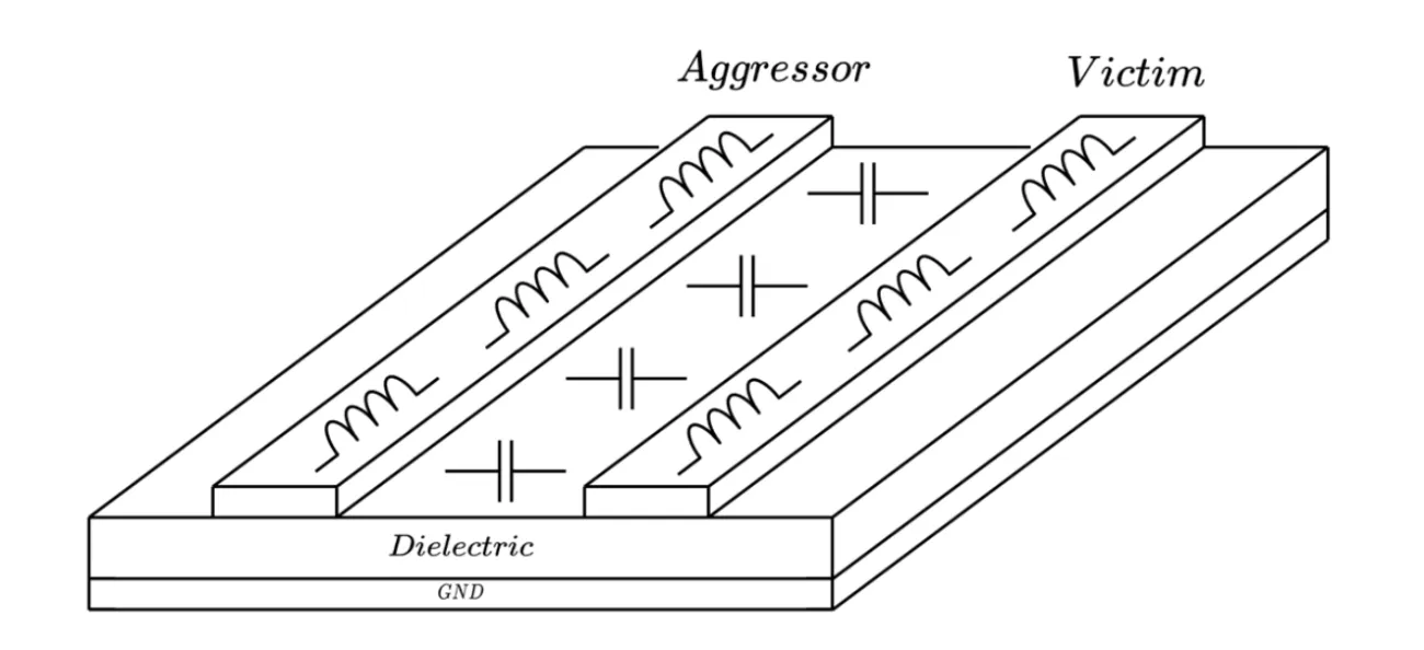
Noise in PCBs arises from multiple sources, including crosstalk, where adjacent signal traces capacitively or inductively couple energy, distorting waveforms. Electromagnetic interference from external fields induces voltages on traces, particularly in unshielded environments with high-frequency clocks. Ground bounce occurs when simultaneous switching of multiple outputs causes voltage fluctuations on ground planes, injecting noise into signals. Reflections from impedance mismatches at vias or connectors create ringing and overshoot, degrading signal edges. Power supply noise couples through decoupling capacitor parasitics, amplifying ripple effects. These mechanisms compound in dense, multilayer boards, demanding proactive mitigation.
Impedance discontinuities, such as abrupt trace width changes or via stubs, reflect signal energy back toward the source, violating timing budgets. Radiated emissions from loop antennas formed by trace-ground pairs exacerbate PCB interference. Thermal effects can shift material dielectric constants, altering characteristic impedance over time. Identifying these root causes through simulation early prevents downstream issues. Electric engineers benefit from modeling these interactions to predict and resolve them before fabrication.
PCB Grounding Techniques for Noise Reduction
Effective PCB grounding techniques form the foundation of PCB noise reduction by providing low-impedance return paths for currents. A solid ground plane on inner layers minimizes loop inductance, reducing ground bounce during simultaneous switching. Splitting planes only when necessary, with stitching vias bridging sections, maintains continuity while isolating analog and digital domains. Star grounding, converging multiple returns to a single point, suits low-speed mixed-signal boards but risks higher inductance in high-speed designs. Prioritize full planes over grids for frequencies above 100 MHz, as grids introduce slots that radiate EMI.
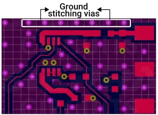
Guard traces adjacent to sensitive signals, tied to ground, absorb stray fields and reduce crosstalk. Decoupling capacitors placed near IC power pins shunt high-frequency noise to ground, with via-in-pad configurations minimizing inductance. Adhering to IPC-2221B guidelines for plane spacing ensures uniform potential distribution. These techniques collectively lower noise floors by 20-40 dB in typical designs, enhancing overall signal integrity.
PCB Shielding Methods to Combat Interference
PCB shielding methods enclose sensitive areas to block external EMI and contain emissions from internal sources. Metal cans or fences around high-speed sections reflect fields, with via fences creating 1/20 wavelength barriers for effective attenuation. Grounded copper pours surrounding traces act as micro-shields, particularly useful for USB or LVDS lines. Enclosure-level shielding integrates with board edges via spring fingers or conductive gaskets for comprehensive protection.
Cavity shielding in multilayer boards dedicates inner layers as shields, grounded on both sides to suppress cavity resonances. For flexible designs, embedded shielding films provide lightweight alternatives without added height. Combining shielding with filtering, such as ferrite beads on I/O lines, addresses both conducted and radiated paths. These methods prove essential in environments with strong ambient fields, like industrial controls.
Layer Stackup and Routing Strategies for Signal Integrity
Optimal layer stackup pairs high-speed signals with adjacent ground planes, achieving stripline or microstrip configurations for controlled impedance. Symmetric stackups prevent warpage and maintain dielectric uniformity, critical per IPC-6012E specifications. Routing minimizes vias by using broadside-coupled differential pairs, preserving balance and common-mode rejection. Length-matched routing for clocks and data buses avoids skew, with serpentine meanders for fine adjustments.
Bend traces at 45-degree angles to reduce reflections at corners, and space singles at least 3x dielectric height from clocks. Buried resistors or series terminations at source ends dampen overshoot without reflections. These strategies integrate seamlessly with grounding and shielding for holistic PCB signal integrity.
Signal Integrity Analysis Techniques
Signal integrity analysis begins with pre-layout impedance profiling using field solvers to target 50 or 100 ohms per trace. Time-domain reflectometry simulates reflections, identifying discontinuities before routing. Eye diagram analysis post-layout verifies margin against bit error rates, incorporating jitter and crosstalk budgets. Frequency-domain sweeps reveal resonances in power distribution networks.
Board-level testing employs TDR/TDT scopes to validate fabricated impedances against simulations. Compliance checks against J-STD-001 for soldering effects ensure production integrity. Iterative analysis refines designs, catching issues missed in initial reviews.
Troubleshooting Common Signal Integrity Issues
When noise persists, inspect return path integrity first, verifying no splits under high-speed signals. Excessive crosstalk signals poor spacing; increase trace-to-trace distance or add ground fills. Ringing indicates under-damping; add source or end terminations matched to Zo. Ground bounce troubleshooting involves adding more decoupling, strategically placed every 1-2 cm. EMI failures often trace to unshielded edges; apply gaskets or fences. Systematic probing with near-field probes localizes sources, guiding targeted fixes.
Conclusion
Mastering PCB signal integrity demands a multifaceted approach, from solid grounding techniques and shielding methods to rigorous analysis. Electric engineers who prioritize impedance control, low-inductance returns, and layered defenses achieve noise-free operation even at multi-Gbps speeds. Integrating these practices early reduces iterations and ensures first-pass success. As designs push higher frequencies, adherence to proven strategies remains paramount for reliable performance.
FAQs
Q1: What is PCB signal integrity, and why is it essential for high-speed designs?
A1: PCB signal integrity ensures signals arrive undistorted, preserving timing and amplitude amid noise and reflections. In high-speed applications, it prevents data corruption from crosstalk or EMI, maintaining protocol compliance. Engineers use it to meet eye diagram specs and minimize bit errors. Proper implementation extends system reliability in dense boards.
Q2: How do PCB grounding techniques contribute to PCB noise reduction?
A2: PCB grounding techniques like full planes and stitching vias provide low-impedance returns, curbing ground bounce and EMI coupling. They minimize loop areas that act as antennas, lowering noise by tens of dB. Decoupling complements them by shunting ripple. Consistent application per design rules yields cleaner power rails.
Q3: What are effective PCB shielding methods for minimizing interference?
A3: PCB shielding methods include via fences and metal cans that reflect fields, attenuating external EMI. Ground pours and cavity layers suppress resonances internally. Combining with routing spacing handles conducted paths too. These suit noisy environments, enhancing signal margins without size penalties.
Q4: How does signal integrity analysis help in PCB design?
A4: Signal integrity analysis tools simulate impedance, crosstalk, and eyes pre- and post-layout, predicting failures early. TDR validates prototypes against models. It guides optimizations like termination, ensuring timing budgets. Regular use cuts debug time and boosts yield.
References
IPC-2221B — Generic Standard on Printed Board Design. IPC, 2012
IPC-6012E — Qualification and Performance Specification for Rigid Printed Boards. IPC, 2017
J-STD-001H — Requirements for Soldered Electrical and Electronic Assemblies. IPC, 2020