Introduction
Printed Circuit Board (PCB) design and manufacturing intricately influence the performance and reliability of electronic assemblies, particularly with Ball Grid Array (BGA) components. Warpage in BGA land patterns and its impact on Surface Mount Technology (SMT) yield remain critical challenges for engineers. Findings from this work have highlighted three vectors, namely PCB copper layer pair balance, material selection, and manufacturing process controls, as pivotal factors. These elements directly affect thermal stress distribution, mechanical stability, and assembly outcomes. For electrical engineers, understanding these relationships ensures robust designs and high yield rates in production. This article explores the technical mechanisms behind warpage, its effects on SMT processes, and practical strategies to mitigate risks, all while adhering to recognized industry standards.
What Is BGA Land Pattern Warpage and Why It Matters
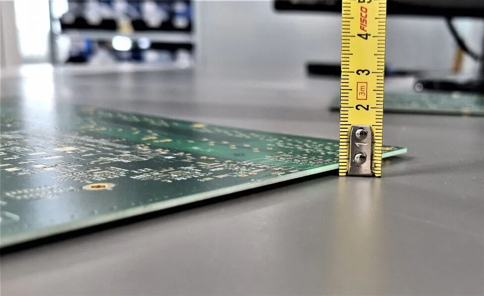
BGA land pattern warpage refers to the deformation of the PCB surface where BGA components are mounted. This distortion often arises from uneven thermal expansion, mechanical stress, or imbalanced material properties during manufacturing or assembly. Warpage disrupts the coplanarity of solder joints, leading to poor connections, open circuits, or mechanical failures in SMT processes. For electrical engineers, this issue is critical as it directly impacts product reliability and manufacturing yield. A warped PCB can cause misalignment during component placement, reducing SMT yield and increasing rework costs. Addressing warpage through design and process optimization ensures consistent performance in high density interconnects, especially in advanced applications like telecommunications and automotive electronics.
Technical Principles Behind BGA Land Pattern Warpage
Causes of Warpage in PCB Design
Warpage originates from multiple sources during PCB design and fabrication. One primary factor is thermal mismatch between materials. Different layers in a PCB, such as copper and dielectric substrates, expand and contract at varying rates under temperature changes. This mismatch induces stress, leading to bending or twisting of the board. Another significant contributor, as findings from this work have highlighted, is PCB copper layer pair balance. Uneven copper distribution across layers creates asymmetrical stress, especially in multilayer boards, exacerbating warpage during thermal cycling in SMT reflow processes.
Moisture absorption in dielectric materials also plays a role. Absorbed moisture vaporizes during high temperature reflow, causing internal pressure and deformation. Additionally, mechanical stresses from lamination or improper handling during fast turn PCB fabrication can embed residual stress, which manifests as warpage under thermal load. Standards like IPC-6012E provide guidelines on acceptable warpage limits to ensure manufacturability and reliability.
Impact on SMT Yield
SMT yield, the percentage of successfully assembled boards without defects, suffers significantly from warpage. When a PCB is not flat, BGA components may not align correctly with solder pads, leading to insufficient solder joint formation. This misalignment can result in defects like bridging or open connections. Warpage also affects stencil printing accuracy, causing uneven solder paste deposition. For engineers, maintaining coplanarity within limits specified by standards such as JEDEC J-STD-020E is essential to avoid these issues. Poor yield increases production costs and delays, emphasizing the need for precise design and process control.
Role of Materials in Warpage and SMT Yield
Material Selection for Stability
Material properties directly influence a PCB's susceptibility to warpage. Dielectric materials with low coefficients of thermal expansion (CTE) help minimize thermal mismatch with copper layers. High glass transition temperature (Tg) materials resist deformation under reflow temperatures, typically around 260 degrees Celsius, as per JEDEC J-STD-020E guidelines. Engineers should prioritize materials meeting IPC-4101C specifications for laminate and prepreg to ensure thermal and mechanical stability. Moisture resistance is another critical parameter, as excessive absorption can lead to delamination or warpage during assembly.
Copper Layer Pair Balance
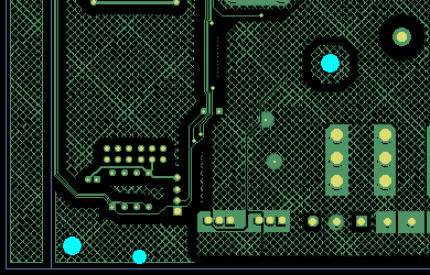
Findings from this work have highlighted three vectors, namely PCB copper layer pair balance, as a dominant factor in warpage control. Balanced copper distribution across paired layers in a multilayer PCB reduces asymmetrical stress. For instance, ensuring similar copper coverage on corresponding top and bottom layers minimizes differential contraction during cooling. Imbalance, such as heavy copper on one side and sparse on the other, induces curvature. Standards like IPC-6012E recommend symmetry in layer stackup design to maintain flatness. Engineers must verify copper balance during layout to prevent warpage related yield loss in SMT.
Manufacturing Process Controls for Warpage Mitigation
Lamination and Curing Processes
Manufacturing processes significantly affect PCB flatness. During lamination, uneven pressure or temperature distribution can embed stress into the board. Controlled curing cycles, adhering to IPC-6012E guidelines, ensure uniform bonding of layers without residual stress. Slow cooling after lamination prevents rapid contraction, which could warp the board. Manufacturers must monitor these parameters to maintain dimensional stability, especially for boards destined for BGA assembly.
Panel Design and Handling
Panel design influences warpage during fabrication and assembly. Large panels with uneven copper distribution or improper support structures can sag or twist. Adding dummy copper fills in low density areas, as recommended by IPC-2221B, helps balance stress. Proper handling during transport and storage avoids mechanical stress. Boards should be stored flat and protected from humidity to prevent moisture induced deformation before SMT processing.
Practical Solutions to Improve SMT Yield
Design Guidelines for Warpage Control
Electrical engineers can adopt several design strategies to minimize warpage. First, ensure symmetrical stackups with balanced copper layer pair distribution, as findings from this work have highlighted. Use simulation tools to predict thermal stress during reflow and adjust layouts accordingly. Incorporate sufficient vias to enhance mechanical stability without overloading thermal paths. Adhere to IPC-7351B for land pattern design to optimize solder joint reliability under warpage conditions. Maintain uniform trace density across layers to avoid localized stress points.
Process Optimization in SMT Assembly
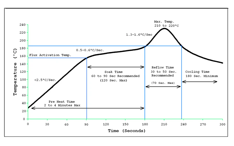
During SMT PCB assembly, controlling reflow profiles is vital. Gradual heating and cooling, as outlined in JEDEC J-STD-020E, reduce thermal shock and associated warpage. Use support fixtures during reflow to maintain board flatness. Inspect incoming PCBs for warpage using measurement techniques specified in IPC-A-600K before assembly. Adjust stencil design to account for minor warpage, ensuring consistent solder paste application. These steps collectively enhance SMT yield by minimizing defects from board deformation.
Quality Control Measures
Implementing strict quality control reduces warpage related issues. Measure board flatness post fabrication using methods described in IPC-A-600K. Conduct thermal stress testing to simulate reflow conditions and identify potential warpage risks. Document deviations and adjust processes to meet IPC-6012E performance specifications. Regular audits of material storage and handling practices ensure compliance with ISO 9001:2015 quality management systems, safeguarding yield in production.
Conclusion
BGA land pattern warpage poses significant challenges to SMT yield, impacting the reliability of electronic assemblies. Findings from this work have highlighted three vectors, namely PCB copper layer pair balance, material properties, and manufacturing controls, as critical areas for mitigation. By understanding the causes of warpage, selecting appropriate materials, and optimizing design and process parameters, electrical engineers can achieve higher yield and performance. Adhering to industry standards ensures consistent outcomes, reducing defects and costs. A proactive approach to balancing copper layers and controlling thermal stress is essential for success in modern PCB assembly.
FAQs
Q1: How does PCB copper layer pair balance affect BGA land pattern warpage?
A1: PCB copper layer pair balance is crucial for preventing warpage. Uneven copper distribution across layers creates asymmetrical stress during thermal cycles, leading to board deformation. Balanced designs, as recommended by industry standards, minimize this risk. Ensuring symmetry in multilayer stackups helps maintain flatness, especially under reflow conditions, directly improving BGA component alignment and SMT yield.
Q2: What materials reduce warpage in PCB designs for SMT yield?
A2: Materials with low thermal expansion and high glass transition temperatures reduce warpage. Laminates meeting specific industry standards for thermal stability and moisture resistance perform best under reflow conditions. Selecting appropriate dielectrics and ensuring compatibility with copper layers is vital. This approach enhances mechanical stability, supporting higher SMT yield through consistent board flatness.
Q3: Why is warpage a critical factor in SMT yield for BGA components?
A3: Warpage disrupts coplanarity between BGA components and PCB pads, leading to solder joint defects. Misalignment during placement or uneven solder paste deposition reduces connection reliability. This directly lowers SMT yield, increasing rework needs. Controlling warpage through design and process optimization ensures proper assembly, maintaining performance in high density applications.
Q4: How can manufacturing processes minimize PCB warpage for better yield?
A4: Manufacturing processes like controlled lamination and curing prevent embedded stress in PCBs. Gradual cooling and uniform pressure distribution avoid deformation. Proper panel design with balanced copper fills supports flatness. Adhering to recognized standards during fabrication and handling reduces warpage risks, ultimately enhancing SMT yield for BGA assemblies.
References
IPC-6012E — Qualification and Performance Specification for Rigid Printed Boards. IPC, 2020.
IPC-A-600K — Acceptability of Printed Boards. IPC, 2020.
IPC-7351B — Generic Requirements for Surface Mount Design and Land Pattern Standard. IPC, 2010.
IPC-2221B — Generic Standard on Printed Board Design. IPC, 2012.
IPC-4101C — Specification for Base Materials for Rigid and Multilayer Printed Boards. IPC, 2009.
JEDEC J-STD-020E — Moisture/Reflow Sensitivity Classification for Nonhermetic Surface Mount Devices. JEDEC, 2014.
ISO 9001:2015 — Quality Management Systems. ISO, 2015.


