Introduction
In the realm of advanced PCB design, high-speed PCB direct imaging emerges as a pivotal technology for fabricating circuits that operate at elevated frequencies. As digital systems push boundaries with faster data rates and denser interconnects, traditional manufacturing methods often fall short in delivering the precision required. Direct imaging, commonly known as LDI for laser direct imaging, addresses these challenges by projecting patterns directly from digital data onto photoresist-coated panels. This process enhances feature resolution and alignment accuracy, making it indispensable for LDI digital circuits. Engineers working on high-speed applications benefit from its ability to maintain signal integrity PCB performance amid shrinking geometries. Factory insights reveal that adopting high-speed PCB direct imaging streamlines production while meeting stringent quality benchmarks.
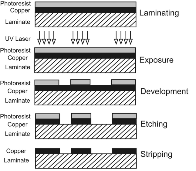
What Is PCB Direct Imaging?
PCB direct imaging involves using a laser system to expose photoresist on a PCB panel according to a digital artwork file, bypassing the need for physical photomasks or films used in conventional photolithography. The laser scans the panel line by line, modulating its intensity to create the desired pattern with high fidelity. This digital approach allows for instantaneous design adjustments without retooling, a significant shift from analog film-based methods prone to distortion. In PCB manufacturing for fast circuits, LDI supports finer line widths and spaces, typically enabling features below conventional limits. The process begins with dry film or liquid photoresist application, followed by precise laser exposure, development, and etching. Its relevance grows in high-volume production where repeatability and yield are paramount.
Related Reading: PCB Direct Imaging for Fine Line PCBs: A Comprehensive Guide
Why Direct Imaging Matters for High-Speed Digital Circuits
High-speed digital circuits demand exceptional signal integrity PCB characteristics, such as controlled impedance, minimal crosstalk, and low insertion loss, which hinge on precise trace geometries. Traditional photolithography introduces variables like film shrinkage, dust artifacts, and alignment errors that degrade these parameters, especially as trace widths approach 50 microns or less. High-speed PCB direct imaging mitigates these issues by eliminating intermediate phototools, ensuring the imaged pattern matches the design intent exactly. For LDI digital circuits operating above gigahertz frequencies, even minor deviations can cause reflections or timing skews. Factory-driven perspectives highlight how LDI reduces scrap rates and rework, aligning with performance specs in IPC-6012E for rigid printed boards. Ultimately, this technology bridges the gap between design complexity and manufacturability in advanced PCB design.
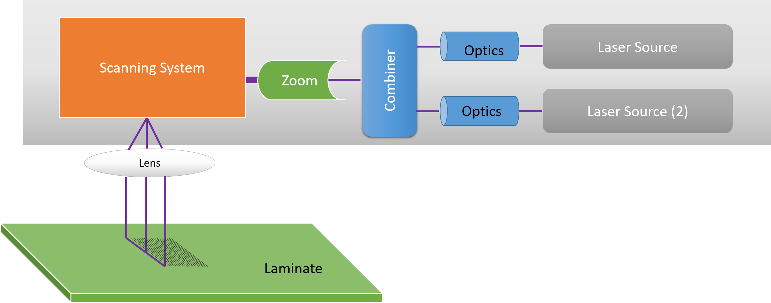
Technical Principles of Laser Direct Imaging
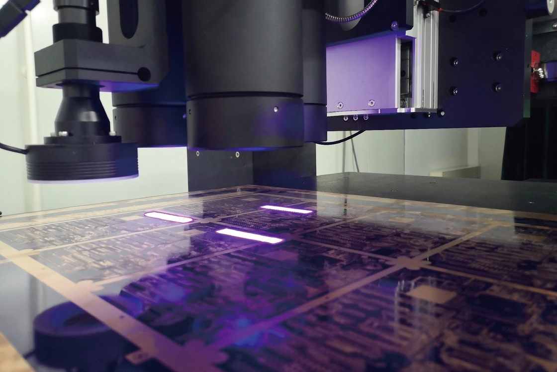
The core mechanism of LDI relies on a high-power UV laser, often operating at 355 nm or 405 nm wavelengths, paired with a spatial light modulator or galvo scanner to direct the beam across the panel. Digital mask data drives the laser, pixelating the image at resolutions exceeding 1000 dpi, far surpassing film contact printing. Exposure occurs in a controlled environment to prevent ambient light interference, with the photoresist responding selectively to the laser energy. Post-exposure, the panel undergoes aqueous development, where unexposed areas dissolve, revealing the pattern for etching. This non-contact method avoids mechanical stress and contamination inherent in stepper or contact aligners. In high-speed PCB direct imaging, vector scanning optimizes throughput for complex patterns, balancing speed and precision.
Key advantages stem from the digital workflow: artwork integrity is preserved from CAD to panel, eliminating scaling errors. Multi-layer registration improves due to fiducial alignment visible to the laser system, critical for stacked vias in dense boards. Thermal management during exposure prevents resist bubbling, ensuring uniform linewidth control. Engineers appreciate how LDI handles panel warpage through adaptive optics, maintaining focus across large formats up to 24 by 24 inches.
Benefits for Signal Integrity in High-Speed PCB Manufacturing
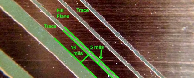
Signal integrity PCB challenges in fast circuits include impedance discontinuities from trace width variations and via stub resonances, both exacerbated by imaging inaccuracies. High-speed PCB direct imaging delivers sub-micron overlay tolerances, enabling consistent 50-ohm traces with etch factors near unity, minimizing undercuts. This precision supports differential pair routing with tight spacing, reducing near-end crosstalk by maintaining uniform coupling. For LDI digital circuits, the absence of film-induced distortions preserves serpentine or length-matched lines essential for skew control. Factory data underscores yield improvements, as LDI patterns exhibit lower Cpk values for critical dimensions compared to photoplots.
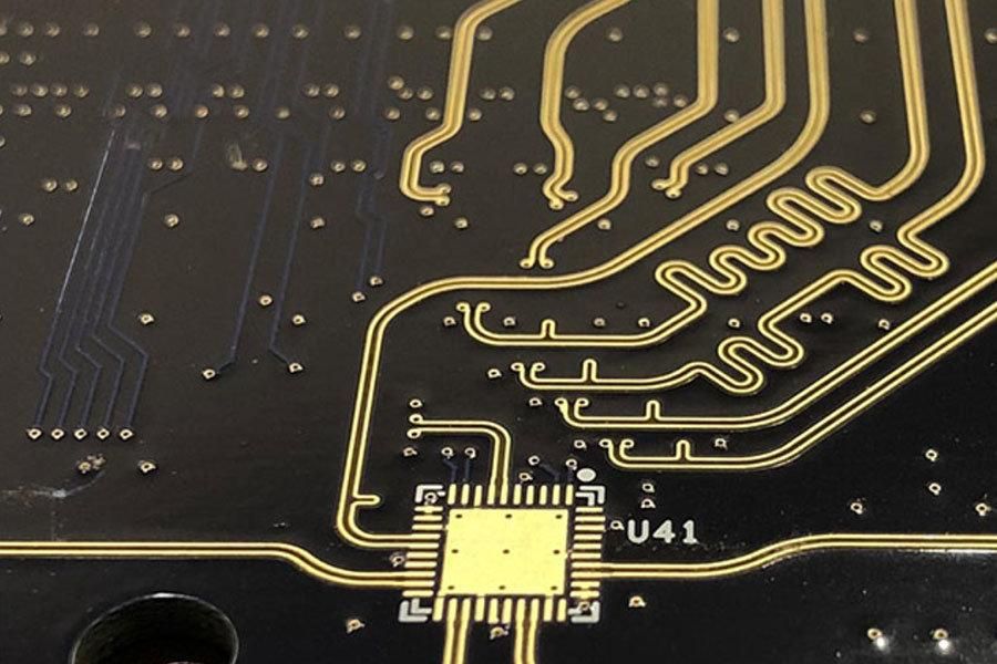
In advanced PCB design, LDI facilitates blind and buried vias with exact landing pads, optimizing return paths and lowering inductance. It excels in HDI structures where microvias demand laser-drilled precision followed by imaged fanouts. Reduced process variation translates to predictable insertion loss, vital for SerDes channels exceeding 25 Gbps. Compliance with IPC-A-600K acceptability criteria becomes routine, as edge roughness and conductor defects plummet. Overall, these attributes fortify signal margins in noisy environments.
Related Reading: Optimizing Via Spacing for Enhanced Signal Integrity in High-Speed PCBs
Best Practices for Implementing Direct Imaging in Fast Circuit Production
To leverage high-speed PCB direct imaging effectively, start with panel preparation: ensure copper surface cleanliness and flatness within 0.75% to avoid defocus. Select photoresists optimized for LDI wavelengths, such as those with high contrast and minimal dose dependency for sharp sidewalls. Calibrate the imaging system daily using traceable standards for dosage and distortion mapping. In PCB manufacturing for fast circuits, incorporate automated optical inspection post-imaging to verify linewidth and registration before etching.
Layer-to-layer alignment demands fiducials at panel corners and center, sized appropriately for the laser's resolution. For multi-up panels, step-and-repeat strategies minimize throughput time while maximizing yield. Engineers should simulate etch compensation in the gerber data to account for isotropic etching, ensuring final geometries match simulations. Adhering to IPC-2221 guidelines for conductor spacing further safeguards signal integrity PCB by preventing shorts in dense routing.
Environment control is crucial: maintain 21-24°C and 45-55% RH to stabilize resist sensitivity. Post-development rinse and dry uniformly to prevent residue bridging. Troubleshooting common issues like incomplete exposure involves dose profiling across the panel. These practices, rooted in factory experience, elevate LDI digital circuits to production readiness.
Insights from Production Applications
In practical deployments for advanced PCB design, LDI shines in backplanes and server boards where high pin counts and dense routing prevail. Factories report seamless transitions from prototype to volume runs, thanks to digital repeatability. One insight is pairing LDI with plasma desmear for vias, enhancing adhesion in high-speed stacks. Challenges like resist lift-off in high-aspect features resolve with optimized developer chemistry. These elements underscore LDI's role in sustaining signal integrity PCB amid evolving demands.
Conclusion
High-speed PCB direct imaging revolutionizes PCB manufacturing for fast circuits by delivering unparalleled precision and flexibility. From eliminating phototool errors to enabling fine-pitch features, LDI fortifies signal integrity PCB in demanding digital applications. Factory-aligned best practices ensure standards compliance and high yields. As advanced PCB design evolves, integrating LDI positions engineers for superior performance and reliability. Embracing this technology future-proofs high-speed designs against tightening tolerances.
FAQs
Q1: What makes high-speed PCB direct imaging superior for signal integrity PCB?
A1: High-speed PCB direct imaging provides exact pattern transfer without film distortions, ensuring uniform trace widths and spaces critical for impedance control. This reduces reflections and crosstalk in LDI digital circuits operating at multi-GHz speeds. Factories achieve better overlay accuracy, aligning with IPC standards for consistent performance. Overall, it minimizes signal degradation from manufacturing variations.
Q2: How does LDI improve PCB manufacturing for fast circuits?
A2: LDI eliminates photomasks, enabling rapid design iterations and finer features for dense routing in fast circuits. It supports precise etching compensation, vital for controlled impedance traces. Production throughput increases due to digital workflows, reducing setup times. This makes it ideal for advanced PCB design requiring high yields and repeatability.
Q3: Why choose direct imaging in advanced PCB design for high-speed applications?
A3: In advanced PCB design, direct imaging offers sub-micron resolution and distortion-free imaging, essential for microvia fanouts and differential pairs. It enhances registration across layers, preserving signal margins. Factories leverage it for HDI boards, meeting tight tolerances without rework. This directly bolsters signal integrity PCB in high-frequency environments.
Q4: What are common best practices for LDI digital circuits production?
A4: Ensure panel flatness and resist compatibility for optimal exposure in LDI digital circuits. Use fiducials for alignment and AOI for verification. Simulate etch effects in artwork to match final dimensions. Maintain controlled environments per standards to avoid defects, ensuring reliable signal integrity PCB outcomes.
References
IPC-6012E — Qualification and Performance Specification for Rigid Printed Boards. IPC, 2017
IPC-A-600K — Acceptability of Printed Boards. IPC, 2020
IPC-2221B — Generic Standard on Printed Board Design. IPC, 2012