Introduction
In modern PCB manufacturing, the demand for finer traces and tighter spaces continues to grow as electronic devices become more compact and performant. Fine line PCB direct imaging, often referred to as LDI fine line manufacturing, represents a pivotal advancement that enables the production of high-density interconnects without the limitations of traditional methods. This technology uses laser beams to project circuit patterns directly onto photoresist-coated panels, bypassing the need for physical films. Engineers designing for high-speed applications or miniaturized assemblies benefit from its precision, which supports complex multilayer boards. This comprehensive guide explores the principles, processes, and PCB manufacturing guidelines associated with direct imaging traces, providing factory-driven insights aligned with industry standards. By understanding these elements, electrical engineers can optimize their designs for reliable production outcomes.
What Is PCB Direct Imaging and Why It Matters for Fine-Line PCBs
PCB direct imaging involves digitally projecting an image onto a photosensitive layer using a controlled laser source, eliminating intermediate phototools. In contrast to conventional contact or projection printing, which relies on artwork films prone to distortion and alignment errors, direct imaging transfers patterns straight from Gerber data. This method shines in fine-line applications, where trace widths and spaces fall into ranges that challenge standard lithography. For electrical engineers working on high-density designs, LDI fine line manufacturing ensures consistent feature sizes across large panels, critical for signal integrity in multilayer stacks. The relevance stems from industry shifts toward smaller components and higher layer counts, where even minor imaging inaccuracies can lead to yield losses or performance issues. Adopting direct imaging aligns production capabilities with evolving PCB design best practices, fostering scalability in manufacturing workflows.
The elimination of films reduces setup times and material costs, making it ideal for prototype iterations and low-volume runs common in engineering development. Factory experience shows that direct imaging maintains pattern fidelity regardless of panel size, a key factor for fine line PCB direct imaging in production environments. Moreover, it supports advanced features like microvias and embedded components, which demand sub-micron registration tolerances.
Technical Principles of Direct Imaging in PCB Manufacturing
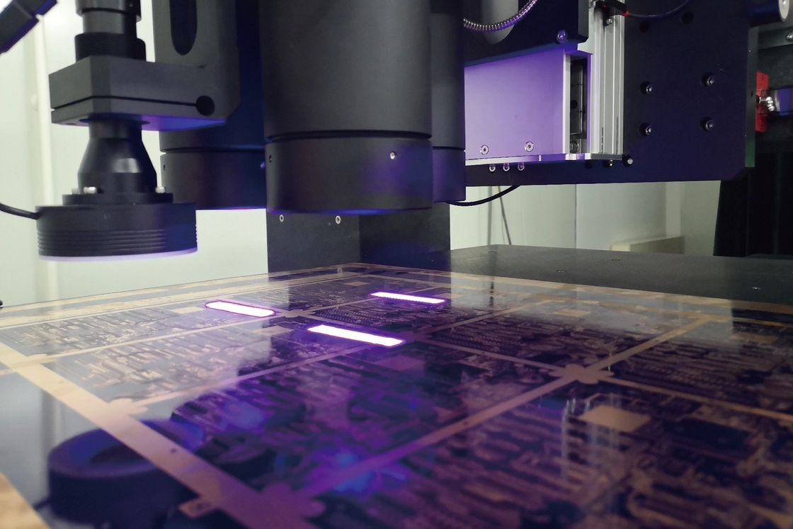
At its core, direct imaging employs ultraviolet lasers to selectively expose photoresist, polymerizing areas that define the copper etch pattern. Systems typically use vector scanning, where the laser beam traces paths defined by vectorized data, or raster scanning for pixel-by-pixel exposure, each suited to different resolutions. Alignment relies on fiducial marks scanned by cameras, achieving overlay accuracies far superior to film-based methods. The laser's wavelength, usually in the 350-450 nm range, matches dry film or liquid resists optimized for high contrast and minimal scattering. Exposure energy must balance to avoid overexposure, which causes linewidth broadening, or underexposure leading to incomplete development. These principles enable direct imaging traces with sharp edges and uniform sidewall profiles post-etching.
In LDI systems, the panel remains stationary or steps incrementally while the laser head moves, allowing imaging of full production panels without splicing. Modulation of laser power and pulse duration fine-tunes resolution, adapting to resist thickness and substrate topography. Factory-driven calibration routines ensure repeatability, with environmental controls like temperature and humidity preventing drift. This technical foundation underpins LDI fine line manufacturing, where minute variations in beam focus directly impact trace integrity.
Related Reading: PCB Direct Imaging: Exploring the Benefits for High Speed Digital Circuits
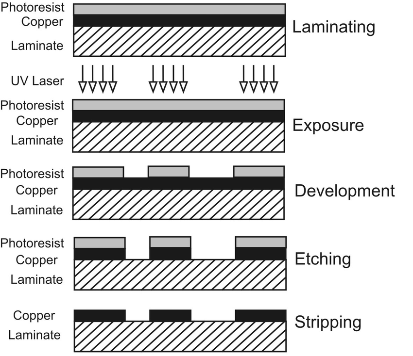
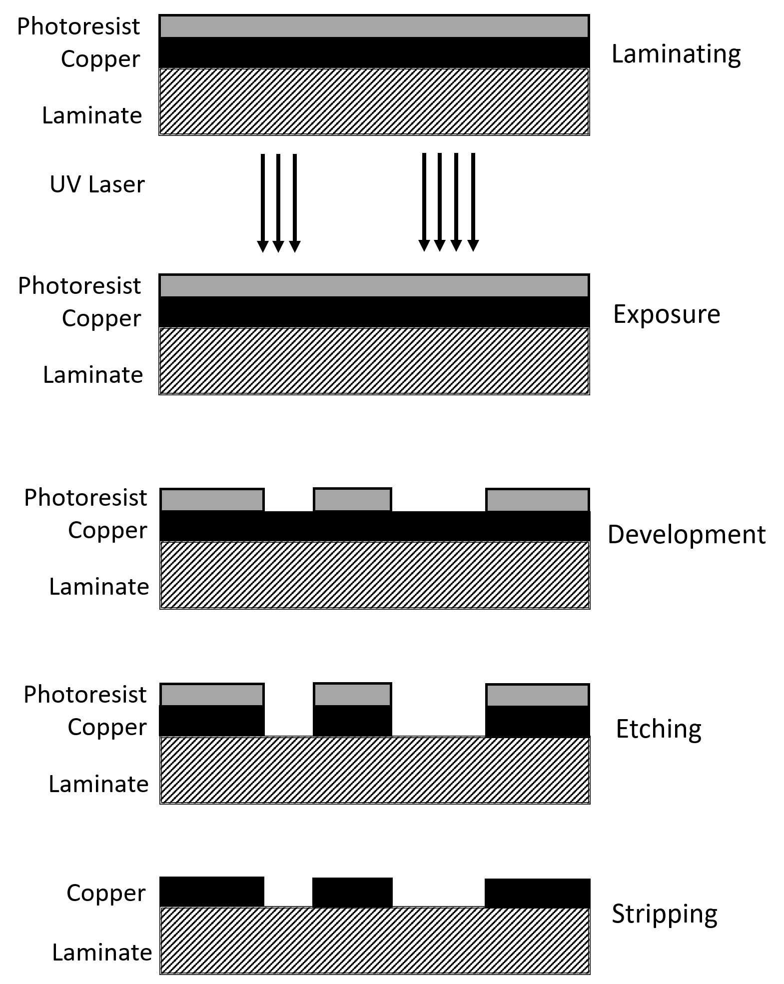
The LDI Process Workflow for Fine-Line PCBs
The process begins with panel preparation, including surface cleaning and lamination of copper foil to dielectric cores for inner layers. A uniform photoresist layer, either dry film laminated under vacuum or liquid spun-coated, covers the copper to protect areas during etching. Digital artwork from the engineer's CAM files loads into the LDI system, where scaling, rotation, and paneling occur automatically. Exposure follows, with the laser delineating traces and pads precisely, followed by aqueous development to remove unexposed resist. Etching transfers the pattern into copper using alkaline or cupric chloride solutions, and stripping cleans the board for subsequent lamination or outer layer processing.
For multilayer fine-line boards, inner layer imaging repeats per core, with registration verified at each stack-up. Outer layers often use tenting resists compatible with LDI for solder mask application later. Post-imaging inspection via automated optical systems confirms line widths and spaces before etching. This workflow, integral to PCB manufacturing guidelines, minimizes handling defects and supports high throughput. Engineers should note that resist adhesion testing precedes production to avoid lift-off during development.
Advantages of Direct Imaging for Fine-Line Manufacturing
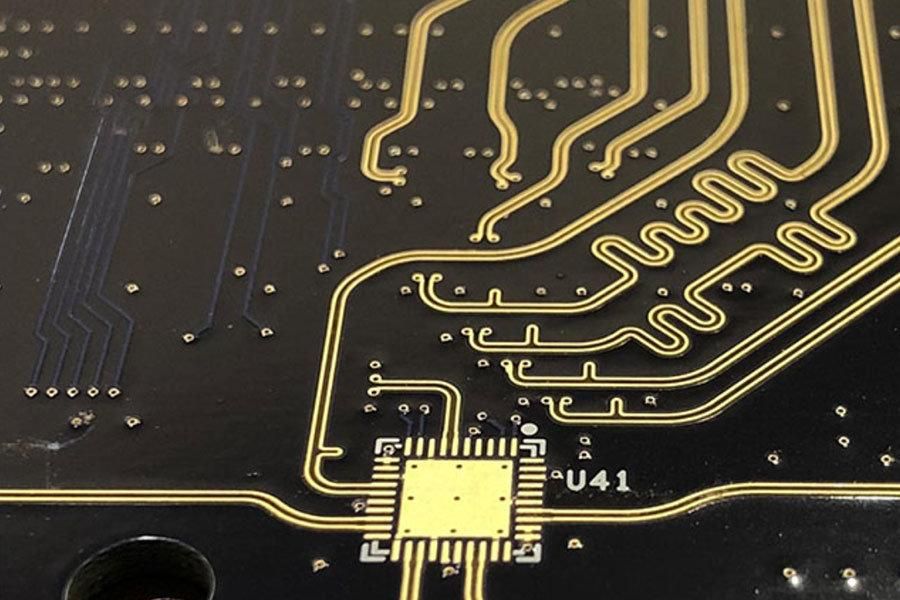
Direct imaging excels in delivering superior resolution and edge definition, crucial for fine line PCB direct imaging where conventional methods falter due to film shrinkage. Without phototools, there's no generational loss in pattern fidelity, ensuring traces match design intent across the panel. Multilayer alignment improves dramatically, as fiducial-based registration compensates for material expansions during lamination. Factories report reduced scrap from misalignment, enhancing yield for complex HDI structures. Additionally, the digital nature allows real-time modifications, accelerating engineering changes without new films.
Cost savings accrue from eliminating film production and storage, particularly beneficial for fine-line prototypes. Environmental benefits include less chemical waste from films, aligning with sustainable PCB manufacturing guidelines. Throughput gains come from automated setups, enabling just-in-time production for electrical engineers under tight schedules. Overall, these advantages position LDI as standard for applications demanding direct imaging traces below traditional limits.
PCB Design Best Practices and Manufacturing Guidelines for LDI
Engineers must prioritize data integrity by exporting Gerber files with high precision apertures and no overlapping primitives, adhering to IPC-6012 qualification specifications for rigid boards. Design rules should account for etch factor, specifying annular rings and clearances to prevent bridging post-development. Smooth trace geometries, avoiding sharp corners that concentrate laser energy, promote uniform exposure. Panel utilization optimizes stepping to minimize edge effects, while fiducials placed symmetrically aid alignment. Substrate flatness below specified tolerances ensures consistent focus depth during scanning.
Resist selection focuses on LDI-compatible films with high sensitivity and adhesion to copper surfaces. Pre-exposure baking removes solvents, enhancing contrast. Factory protocols include plasma cleaning for oxide removal, critical for fine-line adhesion. Exposure dosage calibration per panel lot compensates for thickness variations. Post-etch inspection per IPC-A-600 acceptability criteria verifies conductor width uniformity and void absence. These PCB design best practices integrate seamlessly with LDI fine line manufacturing, bridging design and production.
Common Challenges and Troubleshooting in LDI Fine-Line Production
One frequent issue is haloing around traces, arising from resist scatter or insufficient development, resolved by optimizing exposure energy and spray pressure. Panel warpage during lamination distorts focus, necessitating controlled curing cycles and fixture use. Data errors like aperture mismatches cause imaging artifacts, caught via CAM verification tools. Throughput limitations on large panels stem from scan times, mitigated by multi-beam systems or raster modes for broader coverage.
Related Reading: Minimizing Warpage in Multilayer PCB Manufacturing: Causes and Cures
Resist lift-off signals poor adhesion, often from contamination, addressed through stringent cleaning. Etch undercut in fine spaces results from over-etching, controlled by conveyor speed and chemistry monitoring. Troubleshooting logs in factories track these, with root-cause analysis guiding process tweaks. Electrical engineers benefit from collaborating early on DFM reviews to preempt issues.
Conclusion
PCB direct imaging revolutionizes fine line PCB direct imaging by providing unmatched precision, efficiency, and reliability in manufacturing. From technical laser principles to structured workflows, LDI addresses the demands of modern high-density designs. Implementing PCB manufacturing guidelines and design best practices ensures optimal results, minimizing defects and maximizing yield. As standards like IPC evolve, this technology remains central to advancing PCB capabilities. Electrical engineers equipped with these insights can confidently specify LDI processes for their projects, driving innovation in compact electronics.
FAQs
Q1: What is fine line PCB direct imaging, and how does it differ from traditional methods?
A1: Fine line PCB direct imaging uses laser technology to expose patterns directly on photoresist without films, enabling tighter traces and spaces. Traditional photolithography relies on physical artwork, which introduces alignment errors and resolution limits due to film distortion. LDI offers digital precision and better registration for multilayer boards, making it essential for high-density applications. Factory insights confirm its superiority in yield for complex designs.
Q2: Why is LDI preferred for fine line manufacturing in PCB production?
A2: LDI fine line manufacturing eliminates phototool costs and inaccuracies, supporting precise direct imaging traces critical for HDI and fine-pitch components. It achieves consistent pattern transfer across panels, reducing defects like bridging or opens. Alignment via fiducials ensures interlayer integrity, vital for signal performance. Production scales efficiently without film lead times, aligning with PCB manufacturing guidelines for modern workflows.
Q3: What are key PCB design best practices for direct imaging processes?
A3: PCB design best practices for direct imaging include accurate Gerber data with proper fiducials, smooth trace geometries, and etch-compensated widths to match LDI capabilities. Specify compatible resists and verify panel flatness in stack-up. Avoid data overlaps and include DFM checks for annular rings per standards. These steps ensure manufacturability and high yields in fine-line production.
Q4: How does direct imaging impact quality control in fine-line PCBs?
A4: Direct imaging enhances quality by providing sharp, repeatable traces verifiable via AOI post-exposure. It minimizes variables like film shrinkage, aligning with IPC criteria for conductor integrity. Factories use it to meet tolerances for spaces and pads, reducing rework. Overall, it supports reliable performance in demanding electrical applications.
References
IPC-6012E - Qualification and Performance Specification for Rigid Printed Boards. IPC, 2015
IPC-A-600K - Acceptability of Printed Boards. IPC, 2020