Introduction
In high-reliability PCB manufacturing, precision imaging techniques play a critical role in meeting stringent PCB requirements for sectors like aerospace and medical devices. PCB direct imaging, particularly laser direct imaging (LDI), has emerged as a key process to achieve the fine features and consistent quality demanded by these industries. Traditional photolithography methods struggle with alignment accuracy and feature resolution as designs become denser, making LDI essential for aerospace PCB direct imaging and medical PCB LDI applications. This technology eliminates physical photomasks, reducing defects and enabling rapid adjustments to digital artwork. Engineers designing for mission-critical systems appreciate how quality PCB direct imaging supports compliance with rigorous performance standards. As PCB complexity increases, LDI ensures boards withstand extreme environments without compromising integrity.
What Is PCB Direct Imaging and Why It Matters for High-Reliability Applications
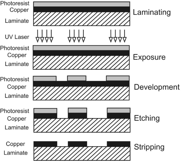
PCB direct imaging refers to a digital exposure process where a laser beam directly patterns photoresist on the PCB substrate using computer-generated data. Unlike conventional photolithography, which relies on physical films or masks that can distort or accumulate defects over time, LDI projects the circuit image pixel by pixel with high fidelity. This method excels in producing fine lines, small vias, and tight spaces necessary for high-density interconnects in modern electronics. For high-reliability PCB manufacturing, LDI matters because it minimizes registration errors across multiple layers, a common failure point in multilayer boards exposed to thermal cycling or mechanical stress.
In aerospace and medical fields, where failure can have catastrophic consequences, LDI addresses stringent PCB requirements by improving yield and traceability. Aerospace systems endure vibration, radiation, and temperature extremes, while medical devices demand biocompatibility and sterilization resistance alongside electrical precision. Quality PCB direct imaging via LDI supports these needs by enabling consistent imaging on varied substrates, including rigid, flex, or rigid-flex configurations. Factory processes benefit from shorter setup times, as changes to designs occur digitally without remaking masks. Overall, LDI elevates manufacturing reliability, aligning with industry expectations for zero-defect production in critical applications.
Technical Principles of Laser Direct Imaging in PCB Fabrication
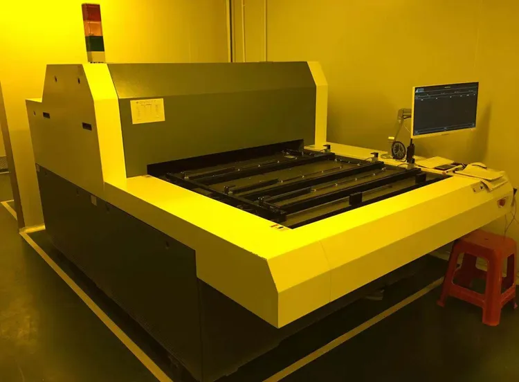
Laser direct imaging operates by scanning a modulated laser beam across a photoresist-coated panel, selectively exposing areas defined by Gerber or ODB++ files. The process begins with applying a thin layer of dry film or liquid photoresist to the copper-clad laminate, followed by precise laser ablation or polymerization. Advanced LDI systems use ultraviolet lasers, typically in the 350-405 nm range, to achieve sub-micron spot sizes for superior resolution. This direct-write approach compensates for panel warpage or scaling distortions in real-time, ensuring accurate overlay between layers.
Key to its effectiveness is the elimination of photomask-related issues like dust particles, stretching, or misalignment, which plague traditional methods. In multilayer PCBs, LDI fiducials and automatic alignment algorithms maintain interlayer registration within tight tolerances required for high-speed signals or dense routing. The technology also supports both positive and negative resists, offering flexibility for different etching processes. For high-reliability applications, these principles translate to fewer process-induced defects, such as shorts or opens, during subsequent plating and etching steps. Engineers value how LDI integrates seamlessly with automated optical inspection, enhancing overall quality control.
Compared to photolithography, LDI provides better depth of focus, allowing uniform exposure even on non-planar surfaces common in thick-core or sequential build-up boards. This is particularly advantageous for aerospace PCB direct imaging, where boards must handle high-frequency signals without signal integrity loss. The digital nature also facilitates step-and-repeat exposure for large panels, optimizing throughput without sacrificing precision.
LDI in Aerospace Applications: Meeting Extreme Demands
Aerospace PCB direct imaging with LDI is vital for fabricating boards that operate in harsh conditions, including rapid pressure changes, high g-forces, and cosmic radiation. These environments demand PCBs with impeccable conductor integrity to prevent migration or delamination under prolonged stress. LDI enables the creation of microvias and blind vias essential for compact avionics and satellite systems, where space constraints drive HDI designs. Factory insights reveal that LDI reduces scrap rates by providing repeatable imaging unaffected by environmental variables like humidity.
Compliance with standards such as IPC-6012E becomes straightforward, as LDI supports Class 3 performance criteria for rigid printed boards, emphasizing electrical, mechanical, and thermal reliability. In practice, aerospace manufacturers use LDI to image inner layers before lamination, ensuring fiducial accuracy for subsequent outer layer alignment. This process mitigates risks like via breakout or plating voids, common pitfalls in high-rel builds. Medical PCB LDI shares similar benefits but focuses on implantables and diagnostics requiring hermetic seals and biocompatible traces.
LDI in Medical Device Manufacturing: Precision for Patient Safety
Medical PCB LDI addresses stringent PCB requirements for devices like pacemakers, imaging equipment, and surgical tools, where precision directly impacts patient outcomes. These applications often involve flexible or rigid-flex boards that must flex without cracking while maintaining signal fidelity. LDI's ability to image on curved or thin substrates ensures uniform resist exposure, critical for fine-pitch components in portable diagnostics. Quality PCB direct imaging here prevents issues like trace thinning, which could lead to intermittent failures during sterilization cycles.
High-reliability PCB manufacturing for medical uses LDI to achieve the tight tolerances specified in IPC-A-600K acceptability criteria, focusing on visual and dimensional standards post-etching. The process supports embedded passives and high-layer counts needed for advanced signal processing in ultrasound or MRI systems. Engineers troubleshoot by leveraging LDI's data logging for process optimization, correlating exposure parameters with yield metrics. Ultimately, LDI enhances traceability, aiding regulatory audits in life-critical sectors.
Best Practices for Implementing LDI in High-Reliability Production
To maximize LDI benefits, start with substrate preparation, ensuring clean, flat panels to optimize laser focus and resist adhesion. Select resists compatible with LDI wavelengths, balancing sensitivity and etch resistance for downstream processes. Implement automated alignment using machine vision to reference fiducials, compensating for any thermal expansion differences between layers.
In high-reliability PCB manufacturing, integrate LDI with electrical test and AOI immediately after development to catch anomalies early. Maintain environmental controls, such as stable temperature and low particulate air, to preserve imaging consistency. For aerospace and medical, validate processes against IPC-6012E qualification tests, including thermal shock and reliability assessments. Document all parameters digitally for full traceability, enabling root-cause analysis if needed.
Multivendor collaboration benefits from standardized digital formats, streamlining design-to-fabrication handoff. Periodic calibration of LDI optics ensures long-term precision, avoiding gradual degradation.
Conclusion
PCB direct imaging through LDI transforms high-reliability PCB manufacturing by delivering unmatched precision, reduced defects, and process flexibility for aerospace and medical applications. It overcomes limitations of traditional methods, enabling finer features and superior registration under stringent PCB requirements. Factory-driven adoption of LDI aligns with standards like IPC-6012E and IPC-A-600K, ensuring boards meet Class 3 reliability. Engineers gain confidence in designs pushing density limits without sacrificing performance. As demands for compact, robust electronics grow, LDI stands as a cornerstone for quality PCB direct imaging in mission-critical sectors.
FAQs
Q1: What advantages does aerospace PCB direct imaging offer over traditional methods?
A1: Aerospace PCB direct imaging with LDI provides superior alignment accuracy and finer resolution without photomask distortions, ideal for high-density avionics. It reduces multilayer registration errors, supporting IPC-6012E Class 3 requirements for vibration and thermal resilience. Factories achieve higher yields and faster prototyping, crucial for iterative designs in space applications. This ensures reliable performance in extreme environments.
Q2: How does medical PCB LDI enhance high-reliability manufacturing?
A2: Medical PCB LDI enables precise imaging on flex substrates, minimizing defects in fine traces for implants and diagnostics. It eliminates mask-related contamination risks, aligning with IPC-A-600K acceptability for clean, durable boards. The digital process supports rapid design changes, vital for customizing patient-specific devices while maintaining stringent quality controls.
Q3: Why is quality PCB direct imaging essential for stringent PCB requirements?
A3: Quality PCB direct imaging via LDI meets stringent PCB requirements by offering real-time distortion correction and sub-micron precision for complex HDI boards. It boosts yield in high-rel production by avoiding phototool wear, common in aerospace and medical. Engineers rely on it for consistent interlayer alignment, ensuring signal integrity and mechanical robustness.
Q4: What role does LDI play in high-reliability PCB manufacturing processes?
A4: LDI streamlines high-reliability PCB manufacturing by directly exposing patterns from digital files, reducing setup time and defects. It excels in multilayer registration for aero-medical boards under IPC standards. Factories integrate it with AOI for defect-free output, supporting zero-fail missions.
References
IPC-6012E — Qualification and Performance Specification for Rigid Printed Boards. IPC, 2017
IPC-A-600K — Acceptability of Printed Boards. IPC, 2020


