Introduction
In modern PCB manufacturing, direct imaging technologies like laser direct imaging (LDI) have become essential for producing high-density interconnects with fine features below 50 microns. These methods offer superior resolution and repeatability compared to traditional contact printing, making them ideal for advanced applications in telecommunications, automotive electronics, and consumer devices. However, PCB direct imaging warped substrates present significant PCB manufacturing challenges, as even minor deviations in flatness can lead to imaging defects, layer misalignment, and reduced yields. Warpage, characterized by bow or twist, arises from inherent material properties and process stresses, complicating the precise focus required for LDI exposure. Engineers must address these issues to maintain quality and efficiency in production lines. This article explores the causes, impacts, and direct imaging solutions to ensure reliable imaging on uneven PCBs.
Understanding PCB Direct Imaging and the Role of Substrate Flatness
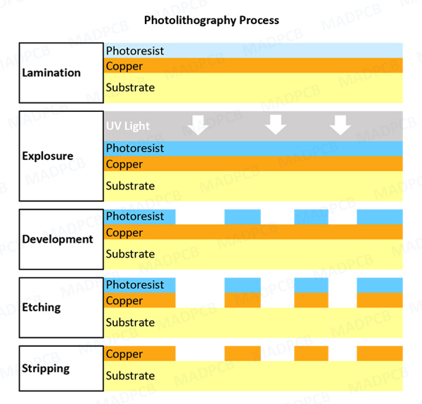
PCB direct imaging, often referred to as LDI, uses a modulated laser beam to project digital circuit patterns directly onto photoresist-coated substrates, eliminating the need for physical photomasks. This process excels in producing sharp images with minimal distortion, supporting trace widths as fine as 25 microns and spaces suitable for high-frequency designs. Substrate flatness is critical because LDI systems maintain a fixed focal depth, typically around 100 to 200 microns, demanding panels lie perfectly planar during exposure. Warped or uneven substrates disrupt this focal plane, causing blurred edges, overexposure in low areas, or underexposure on peaks, which directly impacts feature fidelity.
Industry standards like IPC-A-600 define acceptable bow and twist limits to guide manufacturing tolerances. For surface-mount technology (SMT) boards, the maximum allowable warpage is 0.75 percent of the panel dimension, ensuring compatibility with downstream processes including LDI. Exceeding these limits in PCB direct imaging warped substrates not only compromises imaging quality but also propagates errors into etching and plating stages. Factory engineers prioritize flatness verification early to avoid yield losses that can exceed 10 to 20 percent in severe cases, underscoring why LDI uneven PCB handling is a key focus in process optimization.
Causes of Warpage in PCB Substrates During Manufacturing
Warpage in PCB substrates stems primarily from thermal and mechanical stresses accumulated during lamination and subsequent handling. Coefficient of thermal expansion (CTE) mismatch between copper foil and resin creates internal forces as the stackup cools from press temperatures above 180 degrees Celsius. Uneven copper distribution, such as thicker foils on outer layers or asymmetric innerlayer patterns, exacerbates bowing, with panels often twisting along diagonals. Multilayer boards with high layer counts amplify these effects due to repeated lamination cycles, where core shifts or resin flow imbalances occur.
Process factors further contribute to uneven substrates. Improper cooling rates after pressing lead to residual stresses, while baking for moisture removal can induce additional deformation if humidity gradients exist across the panel. Thick copper constructions, common in power electronics, increase rigidity differences, promoting camel-back warpage where edges lift. Handling thin flex or rigid-flex substrates compounds risks, as their lower stiffness allows greater deflection under gravity or vacuum hold-down.
Test methods outlined in IPC-TM-650, such as 2.4.22 for bow and twist measurement, provide standardized ways to quantify these deformations using fixtures and gauges. Identifying root causes through such protocols enables targeted corrections before imaging.
Key Challenges in LDI Exposure on Warped or Uneven Substrates
When processing LDI uneven PCB substrates, the primary challenge is focal inconsistency, where the laser's depth of field fails to accommodate surface variations exceeding 50 microns. This results in defocused regions with widened traces or incomplete resist hardening, leading to under-etching and opens during development. Layer-to-layer registration errors compound in multilayers, as sequential imaging relies on fiducials that distort under warpage, misaligning vias and pads by several microns.
Yield impacts are profound in high-volume production, with warped panels contributing to scrap rates from imaging defects like spots, halos, or ghosting. These issues necessitate rework or rejection, inflating costs and delaying shipments. Vibration or stage inaccuracies in LDI equipment amplify problems on uneven surfaces, where dynamic focus struggles to track rapid topography changes. Engineers observe higher defect densities at panel edges, where warpage peaks due to fixture constraints.
Direct Imaging Solutions for Handling Warped Substrates
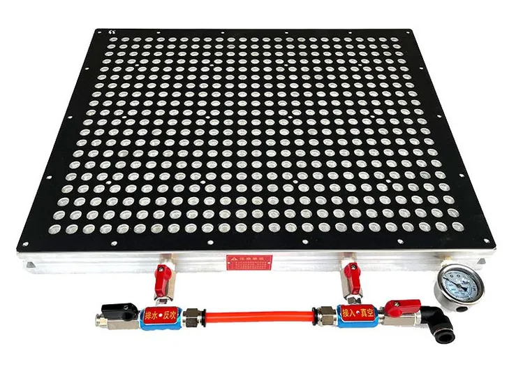
Effective direct imaging solutions begin with mechanical fixturing to minimize substrate deflection during LDI exposure. Vacuum hold-down tables with zoned pressure distribution flatten panels by pulling them against a precision chuck, compensating for up to 100 microns of bow. Custom pin registration jigs align panels rigidly, reducing twist while allowing repeatable loading across production runs. These setups integrate seamlessly with LDI systems, ensuring consistent focal plane alignment.
Advanced LDI technologies incorporate auto-leveling and dynamic focusing mechanisms, scanning substrate topography via laser interferometry before exposure. Multi-beam systems adjust pulse energy and dwell time in real-time, maintaining uniform resist exposure across undulations. Pre-imaging flattening processes, such as controlled baking at 150 degrees Celsius or edge routing to relieve stresses, further enhance flatness. Symmetric panel design, with balanced copper distribution, prevents warpage onset from the design phase.
In-line metrology using IPC-TM-650-compliant tools verifies flatness post-lamination, rejecting outliers before imaging. These combined approaches yield measurable improvements in PCB yields.
Best Practices for Minimizing Warpage and Optimizing LDI Processes
Factory-driven best practices emphasize material selection with matched CTE laminates to curb inherent warpage risks. Optimizing lamination parameters, including uniform pressure above 300 psi and gradual cooling ramps, stabilizes stackups. Post-press handling with supportive carriers prevents deformation during transport to imaging stations. Implementing statistical process control tracks warpage trends, correlating them to supplier lots or press conditions for continuous refinement.
For LDI-specific workflows, engineers calibrate systems daily for focus offset and perform test exposures on warped witness panels. Routing oversized panels to final dimensions before imaging relieves edge stresses, while selective baking equalizes moisture. These steps align with IPC-6012 qualification specs for rigid boards, ensuring performance under thermal excursions.
Training operators on gentle handling and using low-stress dry films further bolsters outcomes. Such protocols transform PCB manufacturing challenges into controlled variables, enhancing overall throughput.
Troubleshooting Common LDI Issues on Uneven Substrates
In production, engineers encounter scenarios where mild warpage evades initial checks, manifesting as inconsistent line widths post-etch. Troubleshooting starts with shadow moiré interferometry to map topography, revealing hotspots tied to copper imbalance. Adjusting LDI dosage curves compensates for depth variations, while retrofitting dynamic focus upgrades older systems.
A typical case involves multilayer HDI panels post-innerlayer lamination, where 0.5 percent twist causes fiducial misalignment. Applying vacuum-assisted pins and pre-exposure flattening resolved registration to under 10 microns, restoring yields. Documenting these interventions via process audits prevents recurrence, embodying factory-driven insights.
Conclusion
Overcoming PCB direct imaging warped substrates requires a multifaceted approach integrating material control, precise fixturing, and advanced LDI capabilities. By adhering to standards like IPC-A-600 and IPC-TM-650, manufacturers mitigate warpage-induced defects, ensuring high-fidelity imaging and superior yields. These direct imaging solutions not only address LDI uneven PCB challenges but also future-proof processes for denser interconnects. Engineers implementing these strategies achieve reliable production, minimizing scrap and accelerating time-to-market.
FAQs
Q1: What are the main causes of warpage affecting PCB direct imaging warped substrates?
A1: Warpage arises from CTE mismatches between copper and resin during lamination cooling, uneven copper distribution, and process stresses like rapid temperature changes. Thick multilayers and improper handling amplify bow and twist. Standards such as IPC-A-600 limit these to 0.75 percent for SMT compatibility. Addressing them early prevents LDI focus issues and maintains imaging precision.
Q2: How does LDI handle uneven PCB substrates in manufacturing?
A2: LDI systems use dynamic focusing and auto-leveling to adjust for surface variations up to 100 microns, scanning topography beforehand. Vacuum fixturing flattens panels during exposure, ensuring uniform laser focus. These features reduce defects like blurring on warped areas. Combined with pre-flattening bakes, they provide robust direct imaging solutions for challenging substrates.
Q3: What best practices improve PCB yields with warped substrates in direct imaging?
A3: Select low-warpage laminates, optimize lamination for symmetric cooling, and employ in-line IPC-TM-650 measurements. Vacuum chucks and symmetric designs minimize deflection before LDI. Calibrating exposure parameters for topography variations further boosts outcomes. These steps tackle PCB manufacturing challenges effectively.
Q4: Why is substrate flatness critical for LDI uneven PCB processes?
A4: Flatness ensures the laser maintains optimal focal depth, preventing defocus that causes trace widening or resist failures. Warped substrates lead to misalignment and yield drops in high-density boards. Standards enforce tolerances to support reliable imaging. Fixturing and metrology uphold these for production success.
References
IPC-A-600K — Acceptability of Printed Boards. IPC, 2020
IPC-6012E — Qualification and Performance Specification for Rigid Printed Boards. IPC, 2017
IPC-TM-650 2.4.22C — Bow and Twist. IPC, 2022


