What is PCB Edge Plating and Why is it Important for Design?
For electrical engineers focused on improving printed circuit board (PCB) performance and reliability, understanding edge plating is crucial. This manufacturing technique applies a conductive metal layer, typically copper, along the board’s perimeter. It serves several vital functions, including providing electrical connections between layers, bolstering grounding, and offering electromagnetic interference (EMI) shielding. These capabilities are especially critical in specialized applications, such as RF designs, where signal integrity and noise reduction are paramount.
The implementation of edge plating directly influences a PCB's performance and longevity. Without proper design and execution, engineers might encounter issues ranging from signal degradation and thermal stress to manufacturing defects. By adhering to established design rules and industry standards, edge plating can significantly enhance board functionality and mitigate common design pitfalls, making it an indispensable tool for advanced PCB layouts.
Why Should Electrical Engineers Consider Edge Plating for PCBs?
Incorporating edge plating into PCB designs offers several compelling advantages, directly impacting a board's electrical and mechanical characteristics.
● Improved Electromagnetic Compatibility (EMC): Edge plating creates a continuous conductive shield around the board’s perimeter, effectively reducing EMI. This benefit is particularly valuable in high-frequency applications where external interference can severely degrade circuit performance.
● Enhanced Grounding Paths: It establishes a low-impedance connection to ground, which is essential for preserving signal integrity, especially in high-speed circuits operating at frequencies above 1 GHz.
● Better Thermal Management: The conductive layer assists in dissipating heat along the board edges, preventing localized hot spots that could potentially harm components or shorten their operational lifespan.
● Increased Mechanical Durability: Edge plating adds structural reinforcement to the PCB, diminishing the risk of damage during handling, assembly, or in challenging operational environments.
● Seamless Enclosure Connectivity: It facilitates direct and reliable contact with metallic enclosures, ensuring that sensitive circuits are fully shielded within their housing.
Grasping these advantages helps engineers make informed decisions on when and how to integrate edge plating into their designs, optimizing both performance and reliability.
What Are the Key Design Rules for PCB Edge Plating?
Designing a PCB with edge plating demands meticulous adherence to specific guidelines to ensure both manufacturability and optimal performance.
Defining Plated Areas
Clearly specify which board edges require plating within your design files. It is not always necessary for all edges to be plated; therefore, precisely mark these regions in your Gerber files or design documentation. Typically, plating is applied to edges where robust shielding or grounding is critical, such as areas adjacent to RF components.
Maintaining Adequate Spacing
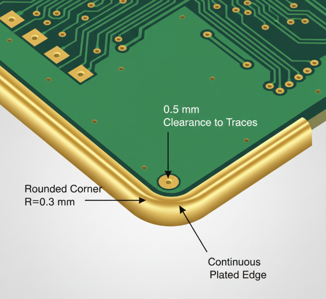
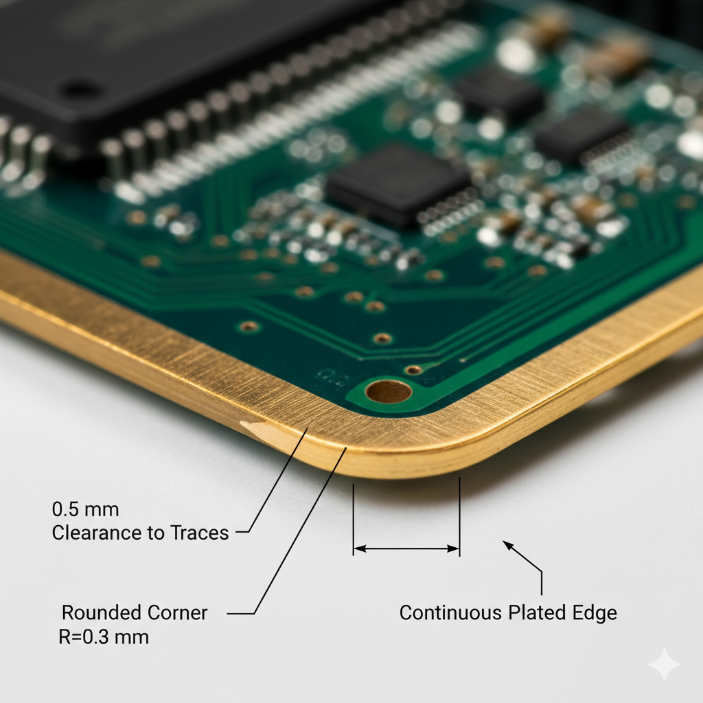
Ensure that no components, traces, or vias are positioned too close to the areas designated for plating. A minimum clearance of 0.5 mm from the board edge is frequently recommended. This precaution prevents potential short circuits or damage during the plating process itself.
Board Thickness Considerations
Edge plating tends to be more effective on PCBs with a thickness of 1.6 mm or greater. Thinner boards may not offer sufficient surface area for the plating to adhere reliably or perform optimally. Always consult your PCB manufacturing supplies regarding their specific capabilities concerning board thickness and plating requirements.
Avoiding Sharp Angles
Sharp corners along the PCB edge can lead to uneven plating deposition and create stress concentration points. To ensure uniform metal application and reduce the likelihood of cracks, incorporate rounded corners with a minimum radius of 0.3 mm into your design.
Specifying Plating Materials
The most common material for edge plating is copper, typically applied with a thickness ranging from 25 to 50 micrometers. This is often followed by a protective surface finish like Electroless Nickel Immersion Gold (ENIG). Clearly defining these material and thickness parameters in your design documentation is crucial for meeting both electrical performance and durability specifications.
What Specifications and Standards Govern PCB Edge Plating?
Adhering to specific technical specifications and industry standards is essential when implementing edge plating. This ensures compatibility with manufacturing processes and the intended end-use applications, leading to high-quality, reliable boards.
Essential Specifications
● Conductive Layer Integrity: The plated edge must form a continuous conductive path without any breaks or gaps. Interruptions can compromise the effectiveness of shielding and grounding. Your design should facilitate uniform plating across all designated edges.
● Surface Finish Alignment: The edge plating's surface finish should be compatible with the overall board finish to prevent corrosion or connectivity issues. For example, if the PCB employs an ENIG finish, the edge plating should also include a complementary nickel and gold layer to maintain material consistency.
● Electrical Resistance Limits: The resistance of the plated edge should be kept low, ideally less than 1 milliohm per square centimeter. This ensures efficient grounding and minimal signal loss. It's advisable to test this parameter during the prototyping phase to validate your design's electrical performance.
● Manufacturing Precision: Edge plating often demands tighter manufacturing tolerances compared to standard PCB features. A typical tolerance for edge plating alignment is ±0.1 mm. Close collaboration with your manufacturer is vital to confirm their capabilities and adjust your design as necessary.
By meeting these detailed specifications, engineers can prevent costly redesigns and ensure the PCB functions precisely as intended in its final application.
Relevant Industry Standards
Compliance with established industry standards for PCB edge plating is fundamental for producing high-quality boards that meet stringent performance and reliability benchmarks.
● IPC-6012: This standard, titled "Qualification and Performance Specification for Rigid PCBs," outlines comprehensive requirements for PCB manufacturing, including specific criteria for edge plating. It covers aspects such as plating thickness, adhesion, and continuity, ensuring that plated edges satisfy critical electrical and mechanical performance demands.
● IPC-A-610: Known as "Acceptability of Electronic Assemblies," this standard, though primarily focused on assembly, includes guidelines pertinent to edge plating as part of overall board quality. It defines acceptable visual and functional criteria for plated edges, such as the absence of voids or delamination, which are key indicators of manufacturing quality.
● IPC-2221: The "Generic Standard on Printed Board Design" provides overarching design guidelines for PCBs, offering recommendations for various board features, including edge plating. It emphasizes appropriate spacing, careful material selection, and structural considerations that are crucial for effective edge plating implementation.
Following these industry standards not only guarantees quality but also enhances clear communication with manufacturers, significantly reducing the potential for errors during the production cycle.
A Practical Checklist for PCB Edge Plating Implementation
To streamline the design and implementation of edge plating, this checklist provides a step-by-step guide for electrical engineers.
● Determine Plating Needs: Identify precisely which edges require plating based on the design’s shielding, grounding, or connectivity requirements.
● Verify Design Documentation: Confirm that Gerber files and associated documentation clearly specify all plating areas and their precise technical parameters.
● Check Component Clearances: Ensure that all components and traces are positioned at least 0.5 mm away from any plated edges to prevent potential interference or shorts.
● Specify Materials and Finishes: Clearly define the plating material (e.g., copper) and the desired surface finish (e.g., ENIG) within your design notes.
● Confirm Board Compatibility: Validate that the PCB's thickness is suitable for edge plating, ideally 1.6 mm or greater.
● Implement Rounded Corners: Design all corners that will be plated with a minimum radius of 0.3 mm to ensure even plating and prevent stress points.
● Engage with Manufacturer: Thoroughly discuss manufacturing tolerances, production capabilities, and any potential additional costs with your chosen manufacturing partner before finalizing the design.
● PCB prototype manufacturing and Test: During prototyping, meticulously measure the electrical resistance and visually inspect the continuity of the plated edges to confirm expected performance.
This comprehensive checklist serves as an efficient reference tool, helping to optimize workflow and minimize potential errors during the critical design phase.
What Challenges Can Arise with PCB Edge Plating and How Are They Addressed?
Despite its numerous benefits, edge plating can present specific challenges during manufacturing and design. Anticipating these issues and having strategies to overcome them is vital for successful implementation.
Addressing Uneven Plating
Uneven deposition of metal can compromise electrical conductivity or weaken shielding effectiveness. To mitigate this, ensure your design avoids excessively sharp corners and overly complex geometries along the plated edges. Collaboration with your manufacturer is also key, as they can optimize the plating process parameters to achieve greater uniformity.
Managing Increased Manufacturing Costs
Edge plating is a specialized process that typically adds to overall production expenses. To control costs, consider limiting plating only to the edges where it is absolutely necessary. Engaging in discussions with your manufacturer about cost-effective options and alternative approaches can also help manage the budget.
Preventing Short Circuits
If components or traces are located too close to a plated edge, there is a significant risk of short circuits. Strict adherence to the recommended clearance of 0.5 mm or more is crucial. Additionally, performing thorough design reviews can help identify and rectify potential issues early in the development cycle, before they become costly manufacturing defects.
By proactively addressing these potential challenges, engineers can ensure a smoother design-to-manufacturing transition and achieve better outcomes for their PCB projects.
Where is PCB Edge Plating Utilized in Today's Electronics?
Edge plating's ability to significantly enhance PCB performance has led to its widespread adoption across various sectors of modern electronics.
● RF and Wireless Applications: For devices such as smartphones and IoT modules operating at frequencies up to 5 GHz, edge plating provides essential EMI shielding, safeguarding signal integrity.
● Automotive Electronics: In vehicle control units and sensor systems, edge plating ensures reliable grounding and efficient thermal management, crucial for components exposed to demanding automotive environments.
● Medical Diagnostic Equipment: High-precision medical devices rely on edge plating to maintain signal integrity and provide robust protection against electromagnetic interference in sensitive diagnostic settings.
● Aerospace and Defense Systems: Edge plating contributes to the robust shielding and enhanced durability required for aerospace electronics, enabling them to withstand extreme conditions and maintain performance.
Understanding these diverse applications helps illustrate the versatility and critical importance of edge plating, guiding engineers in determining its suitability for their specific project requirements.