Introduction
In modern electronics, achieving electromagnetic compatibility (EMC) remains a critical challenge for electrical engineers designing high-speed printed circuit boards (PCBs). As signal frequencies increase and board densities rise, unintended electromagnetic radiation from PCB edges can lead to compliance failures and system interference. PCB edge plating emerges as a proven technique to mitigate these issues by creating a continuous conductive barrier along the board perimeter. This method enhances PCB shielding, reduces edge radiation, and supports overall EMC compliance. Engineers often overlook edge plating during initial design phases, yet its implementation can significantly improve performance without major layout changes. This guide explores the principles, design considerations, and best practices for PCB edge plating EMC optimization, drawing on established engineering approaches.
What Is PCB Edge Plating and Why It Matters for EMC
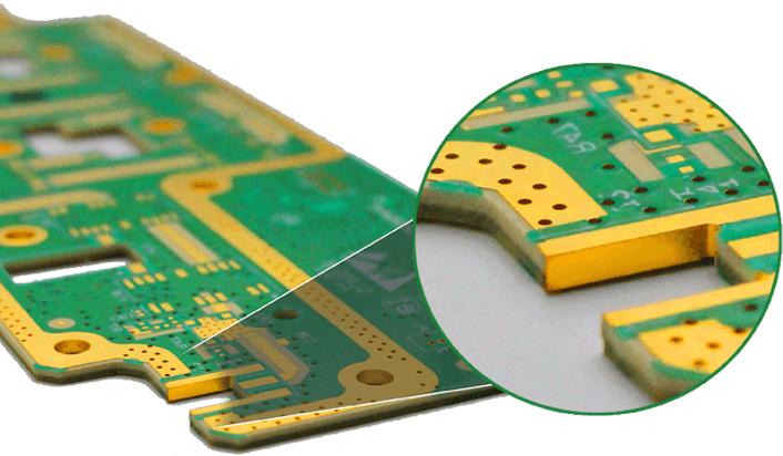
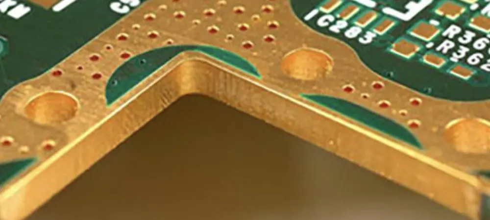
PCB edge plating involves applying a conductive metal layer, typically copper followed by a surface finish like nickel-gold or immersion tin, directly onto the exposed edges of a PCB. This process extends the copper plating from inner layers to the board's periphery, forming a seamless ground connection. Unlike standard via stitching, which leaves gaps, edge plating provides uninterrupted shielding that prevents slots from acting as radiating antennas.
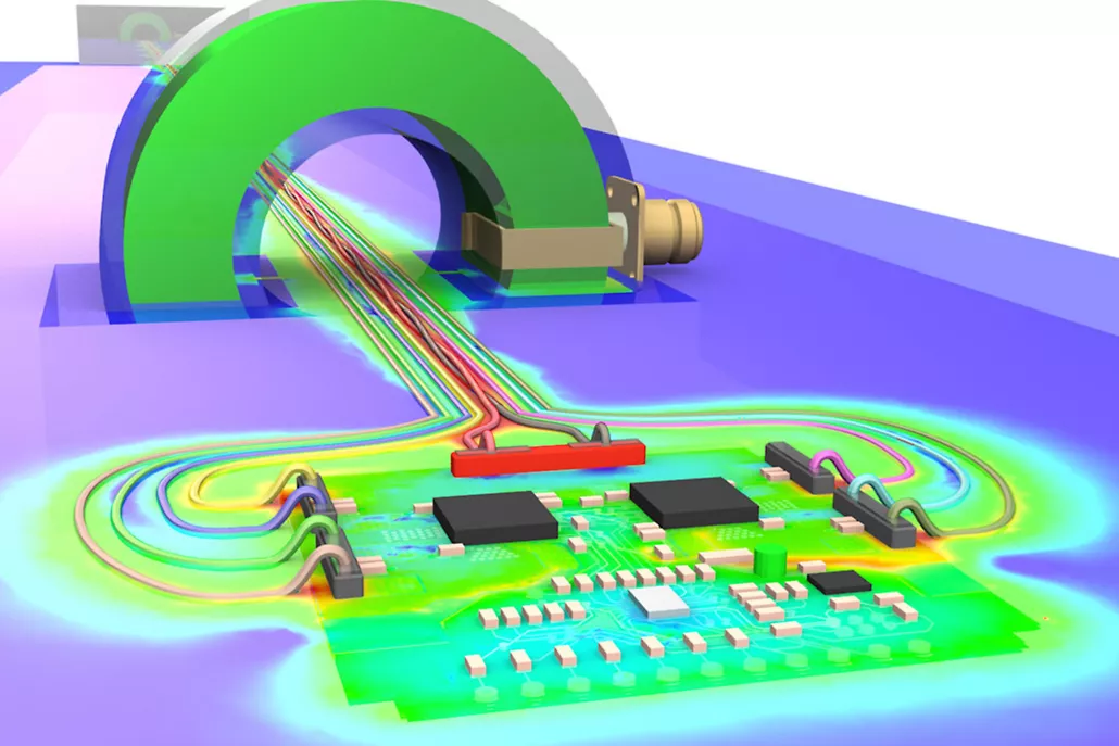
The relevance to electromagnetic compatibility stems from PCB edge radiation mechanisms. Unplated edges in multilayer boards can couple energy from high-speed traces or power planes, radiating emissions that exceed regulatory limits. By grounding the plated edge, return currents flow along the perimeter rather than forming large loops, minimizing far-field radiation. This is particularly vital for applications like telecommunications, automotive electronics, and medical devices where EMC compliance is non-negotiable.
Industry data underscores its impact: edge-plated boards often show measurable reductions in radiated emissions, especially above 1 GHz. For electrical engineers, integrating PCB edge plating EMC strategies early ensures robust designs that pass testing with fewer iterations. It also bolsters mechanical integrity, aiding in connector mating and thermal dissipation.
Technical Principles of PCB Edge Plating for EMC Enhancement
Electromagnetic radiation from PCB edges arises primarily from discontinuities in ground planes and trace imbalances. In a typical multilayer stackup, the board edge interrupts the reference plane, creating a slot radiator that efficiently couples differential-mode and common-mode currents to free space. PCB edge plating addresses this by metallizing the edge, effectively shorting the slot and converting it into a solid ground wall.
The shielding effectiveness relies on the skin effect, where high-frequency currents concentrate on conductor surfaces. A plated edge, tied to the ground plane via extended copper pours, forms a low-impedance path that diverts return currents away from radiating structures. This Faraday cage-like perimeter suppresses both electric and magnetic field leakage, with performance scaling with plating thickness and finish quality.
Consider the geometry: for optimal PCB shielding, the plating must wrap around the bevel or straight-cut edge, typically 0.1 to 0.2 mm thick copper deposit. Simulations show that edge plating outperforms via fences by 10-20 dB in shielding above 500 MHz, as gaps in stitching allow fringing fields to escape. Compliance with IPC-2221 design standards ensures proper clearance from mounting holes and fiducials, preventing plating shorts.
Frequency dependence is key; below 100 MHz, magnetic shielding dominates via loop area reduction, while above, capacitive coupling minimization takes precedence. Engineers must model these effects using field solvers to predict pre-compliance margins. Overall, PCB edge plating electromagnetic compatibility improvements stem from unified ground potential across layers, reducing intra-layer crosstalk.
Practical Solutions and Best Practices for Implementation
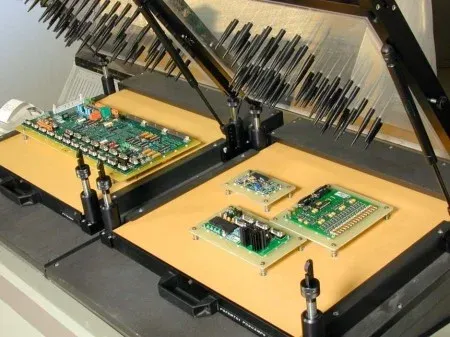
Designing for PCB edge plating requires coordinated efforts between layout, fabrication, and testing phases. Start by defining plated edges in the PCB layout software through copper extension rules to the board outline, specifying full or partial coverage based on emission hotspots. Avoid plating within 0.5 mm of score lines or V-cuts to prevent cracking during depanelization.
Fabrication processes involve routing or milling panels with tabs, plating, then singulating via shear or laser to expose clean edges. Specify HASL, ENIG, or OSP finishes compatible with edge exposure, ensuring adhesion per IPC-6012 qualification criteria. For high-reliability boards, partial depanelization techniques like tab routing allow plating before final cut, maintaining continuity.
Integration with ground planes demands stitching vias every 1/20 wavelength along the edge, though plating reduces this density. Route sensitive traces inward, maintaining 3H spacing (height over ground) to minimize coupling. In stackups, align ground pours on all layers to the edge for maximum shielding efficacy.
Testing validates performance: use near-field probes to scan edges pre-compliance, targeting reductions in E-field peaks. Combine with ferrite beads on I/O lines for hybrid mitigation. Cost considerations favor selective plating on high-risk edges, balancing EMC gains against 10-20% fabrication upcharge.
Troubleshooting Common Issues in PCB Edge Plating for EMC
Engineers frequently encounter voids or delamination in edge plating due to aggressive bevel angles or etchback during desmear. Mitigate by specifying 30-45 degree bevels and verifying panel etch uniformity. Post-plating inspection reveals incomplete coverage; address via fab notes for extended immersion times.
EMC failures post-plating often trace to floating grounds or unconnected inner layers. Verify continuity with flying probe tests, ensuring <1 ohm resistance to primary ground. In high-power designs, thermal expansion mismatches cause cracks; select low-CTE finishes and model stress per IPC guidelines.
Case insights from RF modules show that omitting edge plating on daughter cards led to 15 dB emission spikes at harmonics. Retrofitting via conformal coating failed, but redesign with plated edges achieved compliance on first pass. For backplanes, combine edge plating with castellations for connector shielding.
Signal integrity crosstalk can persist if plating induces resonances; dampen with lossy materials or absorbers. Iterative prototyping with spectrum analysis refines designs, emphasizing plated edges in dense pin fields.
Conclusion
PCB edge plating stands as a cornerstone technique for enhancing EMC performance in demanding designs. By eliminating edge radiation slots and providing robust shielding, it streamlines paths to compliance while improving mechanical reliability. Electrical engineers benefit from its straightforward integration, guided by standards like IPC-2221 and IPC-6012. Prioritize it in high-speed layouts, validate through modeling and testing, and collaborate closely with fabricators. Ultimately, proactive edge plating elevates PCB electromagnetic compatibility, reducing redesign cycles and certification risks.
FAQs
Q1: What is the primary benefit of PCB edge plating for EMC?
A1: PCB edge plating primarily reduces radiated emissions by creating a continuous ground barrier along board edges, preventing slot antenna effects. This shields inner layers from external interference and minimizes internal leakage, which is crucial for high-frequency signals. Implemented per design standards, it can deliver up to 20 dB improvement in shielding effectiveness above 1 GHz while also improving mechanical robustness.
Q2: When should electrical engineers specify PCB edge plating?
A2: Specify edge plating in high-speed digital, RF, or power designs above ~100 MHz, or when pre-compliance scans reveal edge radiation peaks. It is particularly effective on multilayer boards with exposed grounds or dense I/O near edges. Avoid over-specifying on low-frequency boards to control costs, and ensure alignment with stackup and routing strategies.
Q3: How does PCB edge plating compare to via stitching for shielding?
A3: Edge plating typically outperforms via stitching because it provides uninterrupted metal coverage around the board perimeter, eliminating fringing fields that leak through gaps. Via fences can help at lower frequencies but often underperform at GHz ranges. Simulations and measurements commonly show 10-20 dB better shielding with edge plating above 500 MHz, though results are layout dependent.
Q4: What manufacturing considerations apply to PCB edge plating?
A4: Use tabbed panelization so edges can be plated before final singulation, keep plating at least ~0.5 mm away from V-cuts, and specify suitable finishes such as ENIG or HASL for exposed edges. Follow IPC-6012 for adhesion and continuity verification, define edge plating clearly in fab drawings to avoid voids, and consider partial plating to target high-risk edges and manage cost.
References
IPC-2221B — Generic Standard on Printed Board Design. IPC, 2003
IPC-6012E — Qualification and Performance Specification for Rigid Printed Boards. IPC, 2015
IPC-A-600K — Acceptability of Printed Boards. IPC, 2020